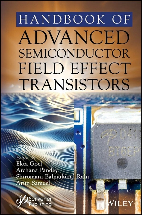
Handbook of Advanced Semiconductor Field Effect Transistors (eBook)
776 Seiten
Wiley-Scrivener (Verlag)
978-1-394-41258-7 (ISBN)
Advance your understanding of semiconductor technology with this indispensable handbook, offering an in-depth look at the modeling, simulation, and fabrication of advanced nanoscale semiconductor field-effect transistors (FETs).
Advanced nanoscale semiconductor field-effect transistors (FETs) represent a pivotal advancement in semiconductor technology, catering to the growing demand for energy-efficient low power electronic devices for emerging applications. This development has significantly impacted the electronics industry, particularly in the design and fabrication of integrated circuits for applications ranging from portable electronics to Internet of Things (IoT) devices. This book provides a comprehensive look at the modelling, simulation, characterization, and fabrication of modern semiconductor FET transistors to improve performance in terms of reduced weight and size, improved subthreshold characteristics and switching performance, and lower power consumption. Handbook of Advanced Semiconductor Field Effect Transistors provides deep insight into the evolving possibilities and challenges of emerging advanced nanoscale FETs. By focusing on the fundamentals of nanoscience and expert knowledge on advanced nanoscale semiconductors, this book serves as a well-rounded guide for novices and professionals looking to innovate in this growing field.
Ekta Goel, PhD is an assistant professor at the National Institute of Technology Warangal. She has published one book chapter and over 50 research articles in peer-reviewed journals and conferences. Her areas of research include modeling and simulation of advanced nanoscale MOS devices, VLSI circuit simulation, photodiodes, and photovoltaic cells.
Archana Pandey, PhD is a senior assistant professor in the Department of Electronics and Communication Engineering at the Jaypee Institute of Information Technology. She has published numerous articles in peer-reviewed international journals and conferences. Her research areas include novel semiconductor devices, FinFETs, device modeling, delay modeling of digital circuit modules, VLSI device-circuit co-design, nanosheet FETs, and FET biosensors.
Shiromani Balmukund Rahi, PhD is an assistant professor at the Mahamaya College of Agriculture, Engineering, and Technology. He has published 25 research papers, two conference proceedings, and 20 book chapters in addition to editing seven books. His work focuses on the development of IoTs for smart applications ultra-low power devices such as tunnel FETs, negative capacitance FETs, and nanosheets.
Arun Samuel, PhD is a professor at the National Engineering College in Kovilpatti, India. He has over 90 publications to his credit and is a lifetime member of the Institute of Engineering and the Institute of Electrical and Electronics Engineers. His research interests include modelling and simulation of multi-gate transistors and tunnel field-effect transistors.
Advance your understanding of semiconductor technology with this indispensable handbook, offering an in-depth look at the modeling, simulation, and fabrication of advanced nanoscale semiconductor field-effect transistors (FETs). Advanced nanoscale semiconductor field-effect transistors (FETs) represent a pivotal advancement in semiconductor technology, catering to the growing demand for energy-efficient low power electronic devices for emerging applications. This development has significantly impacted the electronics industry, particularly in the design and fabrication of integrated circuits for applications ranging from portable electronics to Internet of Things (IoT) devices. This book provides a comprehensive look at the modelling, simulation, characterization, and fabrication of modern semiconductor FET transistors to improve performance in terms of reduced weight and size, improved subthreshold characteristics and switching performance, and lower power consumption. Handbook of Advanced Semiconductor Field Effect Transistors provides deep insight into the evolving possibilities and challenges of emerging advanced nanoscale FETs. By focusing on the fundamentals of nanoscience and expert knowledge on advanced nanoscale semiconductors, this book serves as a well-rounded guide for novices and professionals looking to innovate in this growing field.
Preface
The transistor has become one of the major significant breakthroughs in the electronics field. New techniques of circuit design, miniaturization, and reliability are now emerging, due to the utilization of the transistor and other semiconductor devices. Latest design trends for military equipment have been predominantly towards the use of these devices for the active elements. The purpose of this handbook is to provide the semiconductor players with a reference of reliable, well-designed examples of contemporary devices circuits suitable for use. The brief description about included chapter has been summaries as followings’
In Chapter 1, the field of semiconductor reliability analysis and modeling and provides a detailed examination of the methods and tools used to forecast and improve the durability and efficiency of semiconductor devices. The rapid advancement of semiconductor technology has significantly increased the complexity and functionality of these devices, necessitating the development of sophisticated reliability analysis techniques to meet the changing demands of the industry. The chapter begins with an introduction to the basic principles of semiconductor reliability, including the definitions and importance of reliability metrics and failure mechanisms specific to semiconductor devices. The following sections offer a thorough review of cutting-edge reliability modeling techniques. In this chapter, there are comprehensive discussions on the application of these models in practical settings, underscoring their relevance and effectiveness in forecasting device failures. The particular emphasis is placed on accelerated life testing and its importance in reliability prediction as well as on emerging trends and challenges in the field, such as those introduced by new materials and miniaturization. By merging theoretical knowledge with practical examples, this chapter to provide readers with the knowledge required to understand and address the complexities of semiconductor reliability, enhance their ability to reduce risks, and prolong the functional lifespan of these crucial components.
Chapter 2 describes, the scaling challenges encountered in the nanometer regime with standard single gate bulk MOSFETs are significant because of stern short-channel effects, leading to an exponential rise in the off current and heightened susceptibility to process variations. The double-gate FinFET has emerged as the preferred option among multi-gate transistor architectures, owing to the self-alignment of its two gates, and it also has fabrication steps similar to the existing standard CMOS technology. As the prevalence of embedded systems and mobile devices increases, power consumption has become a paramount concern in contemporary microprocessor designs. Novel latches and flip-flops based on IG-FinFETs, which consume less power and have smaller layout areas, are introduced. To address the challenges associated with the continuous scaling of MOSFETs, fin field-effect transistors (FinFETs) have surfaced as viable alternatives. This enables the ongoing scaling and manufacturing of integrated circuits (ICs) for the creation of smart devices, thereby facilitating smart environments and integrated ecosystems. This chapter provides a concise overview of the fundamental features and operating principles of the FinFETs. It delves into the scaling constraints of mainstream MOSFETs beyond the 22-nm scale owing to short-channel effects (SCEs) and explores scalable alternative FinFET devices for various VLSI circuit design applications. In addition, this chapter highlights the advantages of multiple-gate ultrathin-body FinFET devices. The chapter concludes by addressing the major challenges in the FinFET process, device, and circuit design.
In Chapter 3, the demand for compact, efficient, and low-power electronics has grown exponentially over the last few decades. However, conventional field-effect transistors (FETs) face subthreshold swing (SS) limitations. Thus, modern integrated circuits (ICs) with billions of transistors exhibit high overall power consumption. The negative-capacitance ferroelectric FET (NC-FeFETs) is among the many transistor concepts devised to solve this issue. The NC-FeFET structure is realized by incorporating a ferroelectric material into the FET gate oxide. This modification amplifies the internal voltage near the device channel region, resulting in a steeper SS with a high ION/IOFF ratio, thus reducing power consumption. In this chapter, the fundamentals of NC-FeFETs are discussed in detail. The first section introduces the NC-FeFET and discusses its evolution and operation. The chapter discusses NC-FeFET modeling approaches, applications, performance optimization, and challenges. A comparative analysis of the NC-FeFET with other transistors is also presented. Finally, the chapter concludes with future prospects and research trends highlighting the possibilities of NC-FeFETs as future devices.
Chapter 4 focused on relentless drive towards miniaturization in micro- and nanoelectronics systems has underscored the criticality of power consumption management. This pursuit encounters a formidable obstacle known as Boltzmann tyranny, wherein the generation of a significant drain current necessitates a minimum gate voltage of approximately 60 mV. This imposes a substantial limitation on the scalability of supply voltage in Ultra-Large-Scale Integration circuits, hindering their ability to adapt to the diminishing dimensions of traditional transistors. In response to this pressing challenge, the negative capacitance field-effect transistor has emerged as a promising solution. The NCFET represents a ground-breaking advancement in the field of low-power electronics, offering a promising avenue for overcoming the fundamental limitations of traditional transistor technologies. This novel transistor leverages the unique property of negative capacitance to achieve sub thermal swing and enhance the performance of electronic devices, thereby enabling unprecedented reductions in power consumption. The NCFET operates based on the principle of exploiting ferroelectric materials to induce negative capacitance, resulting in an intrinsic voltage amplification effect. This breakthrough technology effectively addresses the power-efficiency challenges faced by conventional transistors, allowing for the realization of ultralowpower electronic devices without compromising performance metrics. This chapter explores the underlying physics, engineering aspects, design, and simulation methodology of NCFET, highlighting their probable application in circuits. The NCFET has emerged as a transformative technology, promising a paradigm shift towards ultralow-power electronics, highlighting their significance in the ongoing quest for energy-efficient and high-performance electronic devices.
In Chapter 5, Tunnel Field-Effect Transistors have emerged as a promising technology for low power electronic applications due to their steep subthreshold swing and proficiency to operate at lower supply voltages compared to conventional MOSFETs. This chapter provides a comprehensive overview of TFETs, focusing on their fundamental principles, designs, and fabrication techniques. It explores the unique quantum tunneling mechanism that enables TFETs to attain superior performance in terms of power efficiency and scaling. The chapter also discusses the application of TFETs in several domains, including digital electronics, analog and mixed-signal circuits, biosensors, energy harvesting, and communication systems. Furthermore, the potential of TFETs in emerging technologies, such as wearable and implantable medical devices, is discussed, showcasing their role in the future of low power electronics. Future trends and ongoing research efforts aimed at overcoming current challenges and enhancing TFET capabilities are also examined. This comprehensive overview provides valuable insights for researchers, engineers, and industry professionals interested in harnessing the advantages of TFET technology for next-generation electronic applications.
In Chapter 6, MOSFETs have been used in the integrated circuits for a long time. The device dimensions are shrinking continuously due to scaling. A reduction in transistor dimensions is essential for high chip density, low power, increased speed of operation, reduced chip cost, and overall enhanced performance. However, the transistor’s smaller size results in numerous undesirable short channel effects , including hot carrier effect, velocity saturation, drain induced barrier lowering , and reduced gate control over the channel. But for highly scaled devices, the performance of FinFETs is compromised due to various short channel effects which start degrading the device performance. A promising alternative to FinFETs in the near future is the Gate All Around FET (GAA FET), which has excellent short channel performance. GAA FETs have gates on all four sides, in contrast to FinFETs, which have gates around the channel on three sides only. Because of this, the GAA FET has better gate control, has higher drive current, higher ION/IOFF, and is less susceptible to process fluctuations. Also, the short channel performance of GAA FET is better than as compared to FinFET. Multi-gate transistors, such as FinFET and GAA FET, are extremely complex to fabricate. For instance, it is challenging to accurately adjust the fin’s height, width, and inclination angle. In the same way, it is challenging to etch the gate oxide uniformly. Another problem is the oxide and channel contact surface roughness, which can lead to scattering. Another significant problem that might deteriorate the electrical properties of the device is the random...
| Erscheint lt. Verlag | 12.11.2025 |
|---|---|
| Sprache | englisch |
| Themenwelt | Naturwissenschaften ► Chemie |
| Technik ► Maschinenbau | |
| Schlagworte | 2D Materials • Advanced FETs • Channel Engineering • FETs • Gate Engineering • MOSFETs • Nanoelectronic MOS Devices • Nanoscale Devices • Nanoscaled Low Power Semiconductor Devices • Negative Capacitance FETs • Scaling of MOS Devices • Semiconductor Devices • Short channel effects • tunnel field effect transistors • Vertical MOSFETs |
| ISBN-10 | 1-394-41258-4 / 1394412584 |
| ISBN-13 | 978-1-394-41258-7 / 9781394412587 |
| Informationen gemäß Produktsicherheitsverordnung (GPSR) | |
| Haben Sie eine Frage zum Produkt? |
Kopierschutz: Adobe-DRM
Adobe-DRM ist ein Kopierschutz, der das eBook vor Mißbrauch schützen soll. Dabei wird das eBook bereits beim Download auf Ihre persönliche Adobe-ID autorisiert. Lesen können Sie das eBook dann nur auf den Geräten, welche ebenfalls auf Ihre Adobe-ID registriert sind.
Details zum Adobe-DRM
Dateiformat: EPUB (Electronic Publication)
EPUB ist ein offener Standard für eBooks und eignet sich besonders zur Darstellung von Belletristik und Sachbüchern. Der Fließtext wird dynamisch an die Display- und Schriftgröße angepasst. Auch für mobile Lesegeräte ist EPUB daher gut geeignet.
Systemvoraussetzungen:
PC/Mac: Mit einem PC oder Mac können Sie dieses eBook lesen. Sie benötigen eine
eReader: Dieses eBook kann mit (fast) allen eBook-Readern gelesen werden. Mit dem amazon-Kindle ist es aber nicht kompatibel.
Smartphone/Tablet: Egal ob Apple oder Android, dieses eBook können Sie lesen. Sie benötigen eine
Geräteliste und zusätzliche Hinweise
Buying eBooks from abroad
For tax law reasons we can sell eBooks just within Germany and Switzerland. Regrettably we cannot fulfill eBook-orders from other countries.
aus dem Bereich


