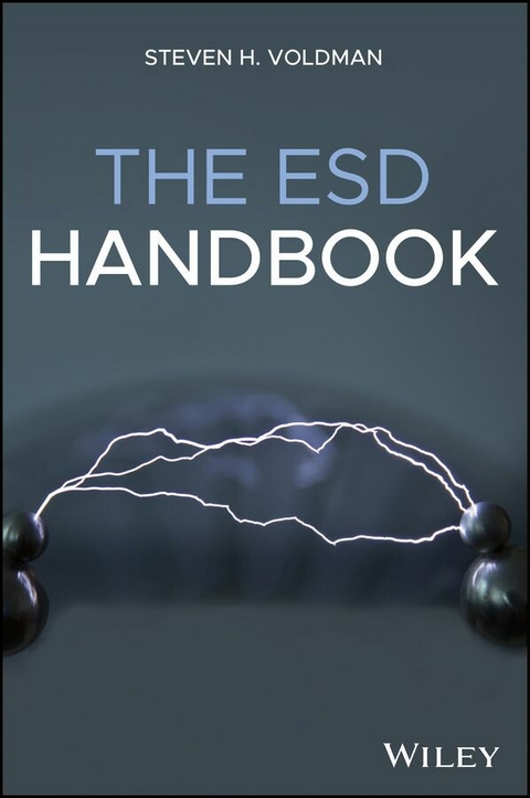
The ESD Handbook (eBook)
1168 Seiten
Wiley (Verlag)
978-1-119-23313-8 (ISBN)
A practical and comprehensive reference that explores Electrostatic Discharge (ESD) in semiconductor components and electronic systems
The ESD Handbook offers a comprehensive reference that explores topics relevant to ESD design in semiconductor components and explores ESD in various systems. Electrostatic discharge is a common problem in the semiconductor environment and this reference fills a gap in the literature by discussing ESD protection. Written by a noted expert on the topic, the text offers a topic-by-topic reference that includes illustrative figures, discussions, and drawings.
The handbook covers a wide-range of topics including ESD in manufacturing (garments, wrist straps, and shoes); ESD Testing; ESD device physics; ESD semiconductor process effects; ESD failure mechanisms; ESD circuits in different technologies (CMOS, Bipolar, etc.); ESD circuit types (Pin, Power, Pin-to-Pin, etc.); and much more. In addition, the text includes a glossary, index, tables, illustrations, and a variety of case studies.
- Contains a well-organized reference that provides a quick review on a range of ESD topics
- Fills the gap in the current literature by providing information from purely scientific and physical aspects to practical applications
- Offers information in clear and accessible terms
- Written by the accomplished author of the popular ESD book series
Written for technicians, operators, engineers, circuit designers, and failure analysis engineers, The ESD Handbook contains an accessible reference to ESD design and ESD systems.
Steven H. Voldman is the first IEEE Fellow for contributions in ESD protection in CMOS, SOI, and Silicon Germanium technology. He has been at the forefront of every major development in semiconductor technology over the past thirty years.
Steven H. Voldman is the first IEEE Fellow for contributions in ESD protection in CMOS, SOI, and Silicon Germanium technology. He has been at the forefront of every major development in semiconductor technology over the past thirty years.
About the Author xxxvii
Acknowledgements xxxix
1 ESD, EOS, EMI, EMC, and Latchup 1
2 ESD in Manufacturing 21
3 ESD Standards 55
4 ESD Testing 65
5 ESD Device Physics 117
6 ESD Events and Protection Circuits 189
7 ESD Failure Mechanism 235
8 ESD Design Synthesis 281
9 On-chip ESD Protection Circuits - Input Circuitry 363
10 On-Chip ESD Protection Circuits - ESD Power Clamps 441
11 ESD Architecture and Floor Planning 491
12 ESD Digital Design 551
13 ESD Analog Design 583
14 ESD RF Design 629
15 ESD Power Electronics Design 681
16 ESD in Advanced CMOS 709
17 ESD in Silicon on Insulator 783
18 ESD in Analog Circuits 821
19 ESD in RF CMOS 865
20 ESD in Silicon Germanium 891
21 ESD in Silicon Germanium Carbon 935
22 ESD in GaAs 951
23 ESD in Bulk and SOI FINFET 971
24 MEMs 979
25 Magnetic Recording 991
26 Photomasks 1003
Appendix Table of Acronyms 1013
A Glossary of Terms - EMC Terminology 1015
B Appendix B. ESD Standards 1017
C Index 1021
D Wiley Series in Electrostatic Discharge (ESD) and Electrical Overstress (EOS) 1055
E ESD Design Rules 1057
F Guard Ring Design Rules 1061
G EOS Design Rules and Checklist 1067
H Latchup Design Rules 1069
I ESD Cookbook 1077
J EOS Cookbook 1079
K Latchup Cookbook 1081
L ESD Design and Release Check List 1087
M EOS Design and Release Checklist 1089
N Latchup Design and Release Checklist 1093
Index 1097
1
ESD, EOS, EMI, EMC, and Latchup
As an introduction, the chapter will first provide a short description of electrostatic discharge (ESD), electrical overstress (EOS), electromagnetic interference, electromagnetic compatibility and latchup. This will be followed by an introduction to the various electrostatic discharge sources and models, followed by an introduction to electrical overstress issues, and the other areas. Electrostatics has been a subject of interest for many years [1–15].
1.1 Electrostatic Discharge (ESD)
1.1.1 What Do You Mean by the Term “Electrostatic Discharge”?
ESD is a subclass of EOS and may cause immediate device failure, permanent parameter shifts and latent damage causing increased degradation rate [15–76]. It has at least one of the following three components: localized heat generation, high current density and high electric field gradient; in addition, there is the prolonged presence of currents of several amperes that transfer energy to the device structure which can cause damage.
ESD is addressed on semiconductor components through ESD circuits, chip architecture and design. During ESD events, ESD failure mechanisms occur in the semiconductor devices. In ESD semiconductor chip design, the ESD design discipline is customized to different application spaces, such as ESD digital design, ESD radio frequency (RF) design, and ESD analog design. With semiconductor component scaling, and both evolutionary and revolutionary changes, ESD devices and design must also evolve.
ESD test practices have evolved for both components and systems over the last 30 years. ESD standard practices, and standards, have evolved with the changes of semiconductor components and new issues. For systems, new issues such as cable discharge events, IEC 61000-4-2 system events and the human metal model have occurred.
1.2 Human Body Model (HBM)
1.2.1 Why Do We Have a Human Body Model?
1.2.1.1 What Does it Characterize?
A fundamental model used in the ESD industry is known as the human body model (HBM) pulse. The model was intended to represent the interaction of the electrical discharge from a human being, who is charged, with a component, or object. The model assumes that the human being is the initial condition. The charged source then touches a component or object using a finger. The physical contact between the charged human being and the component or object allows for current transfer between the human being and the object. A characteristic time of the HBM event is associated with the electrical components used to emulate the human being. In the HBM standard, the circuit component to simulate the charged human being is a 100 pF capacitor in series with a 1500 Ω resistor. This network has a characteristic rise time and decay time. The characteristic decay time is associated with the time of the network
where RHBM is the series resistor and CHBM is the charged capacitor. This is a characteristic time of the charged source. Figure 1.1 shows the HBM pulse waveform
Figure 1.1 Human body model (HBM) pulse waveform.
Figure 1.2 Human body model equivalent circuit model.
Figure 1.2 shows the equivalent circuit model. The equivalent circuit model includes a capacitor and resistor element. In the HBM standard, the circuit component to simulate the charged human being is a 100 pF capacitor in series with a 1500 Ω resistor.
The source contains a 100 pF capacitor in series with a 1500 Ω resistor.
1.3 Machine Model (MM)
1.3.1 What is the Purpose of the Machine Model?
1.3.1.1 How is it Different from the Human Body Model?
Another fundamental model used in the semiconductor industry is known as the machine model (MM) pulse. The MM event was intended to represent the interaction of an electrical discharge from a conductive source, which is charged, with a component, or object. The model assumes that the “machine” is charged as the initial condition. The charged source then touches a component or object. In this model, an arc discharge is assumed to occur between the source and the component or object, allowing for current transfer between the charged object and the component or object. A MM characteristic time is associated with the electrical components used to emulate the discharge process. In the MM standard, the circuit component is a 200 pF capacitor with no resistive component (Figure 1.3). An arc discharge fundamentally has a resistance on the order of 10–25 Ω. The characteristic decay time is associated with the time of the network
where R is the arc discharge resistor and C is the charged capacitor. This is a characteristic time of the charged source.
Figure 1.4 shows an example of the machine model (MM) pulse waveform. Without a large resistor element, the MM pulse waveform is a weakly damped oscillation, whose waveform oscillates from a positive to negative polarity. Additionally, the peak current of the MM pulse waveform is significantly higher than a HBM pulse waveform. It is the feature of higher peak current, as well as polarity transitions, that makes this ESD test more difficult to achieve the desired specification objectives.
1.4 Cassette Model
1.4.1 Why Do We Have a Cassette Model? What Does it Represent?
The Cassette Model (CM), also known as the Charged Cassette Model (CCM), is a recent model associated with consumer electronics. In consumer electronics there are many applications where a human plugs a small cartridge or cassette into an electronic socket. These applications are evident in popular electronic games. The cassette model is of interest to corporations in the “game industry.” In today’s electronic world, there are many palm size electronic components that must be socketed into a system for non-wireless applications. To verify the electronic safety of such equipment, the cassette itself is assumed as a charged source. The “cassette model” assumes a small capacitance, and negligible resistance. This model is equivalent to a MM-type current source with a much lower capacitor component. The model assumes the resistance of an arc discharge, and a capacitance of 10 pF [10]. In the CCM, the customer objectives for this model are on the order of 600 V.
Figure 1.3 Machine model (MM) equivalent circuit model.
Figure 1.4 Machine model pulse.
1.5 Charged Device Model (CDM)
1.5.1 What is the Charged Device Model?
1.5.1.1 Why is it Important?
A Quality and Reliability team wanted to start requiring the “charged device model” standard as part of the qualification. The Design team, who did not want to risk the release of their ASIC library refused to do it. The Quality and Reliability team gave up the fight.
The qualification test vehicle with all the circuitry for the qualification was manufactured, diced and then packaged oversees in Japan. When the parts were returned, there were four pins that were failing – two on the top, and two on the bottom. One hundred percent of the hardware had this failure, and the circuit design qualification failed due to lack of hardware. The area covered by the two top pins and two bottom pins was about the size of a manufacturing person’s finger.
Figure 1.5 CDM test equipment. Source: Steven H Voldman.
In the CDM process, a semiconductor chip is placed “bug up” with the backside of the semiconductor chip on an insulating surface. The semiconductor chip is charged through the ground pin. The ground chip is removed, leaving the chip fully charged on the insulating surface. A pogo pin is then placed over a signal pad, and dropped onto the pin (or bond pad, or solder ball) where the semiconductor chip is discharged through to a 1 Ω ground connection.
Figure 1.5 is an example of a commercial CDM tester used in the qualification of semiconductor chips. The commercial CDM testers are designed in compliance with the CDM test standards [54].
1.6 Transmission Line Pulse (TLP)
1.6.1 Why was the TLP Model Introduced?
1.6.1.1 Why is it So Valuable for Circuit Designers and ESD Engineers?
Transmission line pulse (TLP) testing has seen considerable growth in the ESD discipline. In this form of ESD testing, a transmission line cable is charged using a voltage source. The TLP system discharges the pulse into the device under test (DUT). The characteristic time of the pulse is associated with the length of the cable. The pulse width of a TLP is a function of the length of the transmission line and the propagation velocity of the transmission line.
TLP systems are designed in different configurations. TLP system configurations include Current source, Time Domain Reflectometry (TDR), Time Domain...
| Erscheint lt. Verlag | 25.3.2021 |
|---|---|
| Sprache | englisch |
| Themenwelt | Naturwissenschaften ► Physik / Astronomie ► Elektrodynamik |
| Technik ► Elektrotechnik / Energietechnik | |
| Schlagworte | Circuit Theory & Design • Electrical & Electronics Engineering • Elektrotechnik u. Elektronik • Halbleiter • Leistungselektronik • Power Electronics • Schaltkreise • Schaltkreise - Theorie u. Entwurf • semiconductors |
| ISBN-10 | 1-119-23313-5 / 1119233135 |
| ISBN-13 | 978-1-119-23313-8 / 9781119233138 |
| Informationen gemäß Produktsicherheitsverordnung (GPSR) | |
| Haben Sie eine Frage zum Produkt? |
Kopierschutz: Adobe-DRM
Adobe-DRM ist ein Kopierschutz, der das eBook vor Mißbrauch schützen soll. Dabei wird das eBook bereits beim Download auf Ihre persönliche Adobe-ID autorisiert. Lesen können Sie das eBook dann nur auf den Geräten, welche ebenfalls auf Ihre Adobe-ID registriert sind.
Details zum Adobe-DRM
Dateiformat: EPUB (Electronic Publication)
EPUB ist ein offener Standard für eBooks und eignet sich besonders zur Darstellung von Belletristik und Sachbüchern. Der Fließtext wird dynamisch an die Display- und Schriftgröße angepasst. Auch für mobile Lesegeräte ist EPUB daher gut geeignet.
Systemvoraussetzungen:
PC/Mac: Mit einem PC oder Mac können Sie dieses eBook lesen. Sie benötigen eine
eReader: Dieses eBook kann mit (fast) allen eBook-Readern gelesen werden. Mit dem amazon-Kindle ist es aber nicht kompatibel.
Smartphone/Tablet: Egal ob Apple oder Android, dieses eBook können Sie lesen. Sie benötigen eine
Geräteliste und zusätzliche Hinweise
Buying eBooks from abroad
For tax law reasons we can sell eBooks just within Germany and Switzerland. Regrettably we cannot fulfill eBook-orders from other countries.
aus dem Bereich


