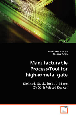
Manufacturable Process/Tool for high-k/metal gate
Dielectric Stacks for Sub-45 nm CMOS
Seiten
2008
VDM Verlag Dr. Müller
978-3-8364-8156-4 (ISBN)
VDM Verlag Dr. Müller
978-3-8364-8156-4 (ISBN)
- Titel nicht im Sortiment
- Artikel merken
Off state leakage current related power dominates the CMOS heat dissipation problem of state of the art silicon integrated circuits. In this study, this issue has been addressed in terms of a low-cost single wafer processing (SWP) technique using a single tool for the fabrication of high- dielectric gate stacks for sub-45 nm CMOS. A system for monolayer photoassisted deposition was modified to deposit high-quality HfO2 films with in-situ clean, in-situ oxide film deposition, and in-situ anneal capability. The system was automated with Labview 8.2 for gas/precursor delivery, substrate temperature and UV lamp. The gold-hafnium oxide-aluminum (Au-HfO2-Al) stacks processed in this system had superior quality oxide characteristics with gate leakage current density on the order of 1 x 10-12 A/cm2 @ 1V and maximum capacitance on the order of 75 nF for EOT=0.39 nm. Achieving low leakage current density along with high capacitance demonstrated the excellent performance of the process developed. Detailed study of the deposition characteristics such as linearity, saturation behavior, film thickness and temperature dependence was performed for tight control on process parameters. Using Box-Behnken design of experiments, process optimization was performed for an optimal recipe for HfO2 films. UV treatment with in-situ processing of metal/high- dielectric stacks was studied to provide reduced variation in gate leakage current and capacitance. High-resolution transmission electron microscopy (TEM) was performed to calculate the equivalent oxide thickness (EOT) and dielectric constant of the films. Overall, this study shows that the in-situ fabrication of MIS gate stacks allows for lower processing costs, high throughput, and superior device performance.
Dr.Aarthi Venkateshan completed PhD from Clemson University, SC. Her doctoral research included developing a manufacturable process/tool for high performance metal/high-k gate dielectric stacks for sub-45 nm CMOS & related devices. She held Applied Materials Graduate Fellowship Award 2004-2007.
Dr.Rajendra Singh is Houser D Banks Professor at Holcombe Department of Electrical & Computer Engg, Clemson Univ. In the last 15 years, his research contributions have been primarily in the field of rapid thermal processing, and manufacturing of silicon integrated circuits and solar cells.
| Sprache | englisch |
|---|---|
| Maße | 150 x 220 mm |
| Gewicht | 284 g |
| Themenwelt | Technik ► Elektrotechnik / Energietechnik |
| ISBN-10 | 3-8364-8156-1 / 3836481561 |
| ISBN-13 | 978-3-8364-8156-4 / 9783836481564 |
| Zustand | Neuware |
| Haben Sie eine Frage zum Produkt? |
Mehr entdecken
aus dem Bereich
aus dem Bereich
DIN-Normen und Technische Regeln für die Elektroinstallation
Buch | Softcover (2023)
Beuth (Verlag)
CHF 119,95
Kolbenmaschinen - Strömungsmaschinen - Kraftwerke
Buch | Hardcover (2023)
Hanser (Verlag)
CHF 69,95


