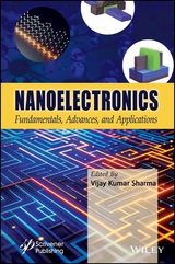
Nanoelectronics (eBook)
857 Seiten
Wiley-Scrivener (Verlag)
978-1-394-27517-5 (ISBN)
Nanoelectronics is an essential resource for anyone looking to stay at the forefront of innovation, as it thoroughly explores cutting-edge methodologies and design principles for ultra-nanoscale technology.
Modern research aims to make devices more efficient so that next-level systems will be energy-efficient, have faster operating speeds, and occupy minimal space. Traditional methods for the implementation of systems are approaching their fundamental limitations. The field of ultra-nanoscale technology is a prime choice for researchers to work and develop technologies for future systems. The advantages of the ultra-nanoscale field are low-dimensional and high-speed implementation with a focus on high levels of functional integration.
Nanoelectronics: Fundamentals, Advances, and Applications comprehensively covers both introductory and advanced-level ideas and methodologies, which support future system designs in ultra-nanoscale technologies. The merits and challenges of different technological devices and systems are also discussed in depth. This book focuses on design and techniques for the next generation of intelligent systems, making it an essential resource for novices and experts exploring this innovative technology.
Vijay Kumar Sharma, PhD is an assistant professor in the School of Electronics and Communication Engineering at Shri Mata Vaishno Devi University. He is published widely in journals and conferences of repute and has authored many book chapters and patents. His research interests are in the area of low-power circuit design.
Nanoelectronics is an essential resource for anyone looking to stay at the forefront of innovation, as it thoroughly explores cutting-edge methodologies and design principles for ultra-nanoscale technology. Modern research aims to make devices more efficient so that next-level systems will be energy-efficient, have faster operating speeds, and occupy minimal space. Traditional methods for the implementation of systems are approaching their fundamental limitations. The field of ultra-nanoscale technology is a prime choice for researchers to work and develop technologies for future systems. The advantages of the ultra-nanoscale field are low-dimensional and high-speed implementation with a focus on high levels of functional integration. Nanoelectronics: Fundamentals, Advances, and Applications comprehensively covers both introductory and advanced-level ideas and methodologies, which support future system designs in ultra-nanoscale technologies. The merits and challenges of different technological devices and systems are also discussed in depth. This book focuses on design and techniques for the next generation of intelligent systems, making it an essential resource for novices and experts exploring this innovative technology.
1
Gaussian Doped SOI Junctionless FinFET: A Study of RDF Variability and Parametric Sensitivity
Milad Mehmood Zargar1, Md. Waseem Akram1, Umayia Mushtaq1*, Nazida Ansari1, Sana Fatima1 and Dipak Kumar Singh2
1Dept. of E & C, Jamia Millia Islamia, New Delhi, India
2Dept. of ECE, National Institute of Technology Patna, Patna, India
Abstract
The advent of modern-day technology has brought with itself a plethora of design problems. The charming attributes of MOS technology are proving to be ephemeral as the chip makers of present day are over obsessed with the objective of scaling. This has unveiled the shortcomings and limitations of the conventional inversion mode devices, which has compelled designers to contemplate sophisticated technologies. Among the ultra-modern devices that have divulged in recent past include neoteric yet virgin technology, junctionless transistors, which has paved the way for simpler fabrication processes. Lesser design complexity, low thermal budget, lack of junctions to avoid formation of abrupt P–N junctions are some of the appealing features of this novel device. Regardless of the unique characteristics of this device, it has to be investigated against various effects including variability, before fabrication on a large scale. As such, this work deals with the functioning of the device when there is a variation in the dopant atoms’ number and location. This type of variability, also called as random dopant fluctuation (RDF), is a significant source of unpredictability in the current environment. Since RDF largely effects these devices, our prior concern was to develop a distinctive doping pattern in these devices, so that the effective degenerative effect of RDF is reduced. The doping scheme suggested in this work corresponds to Gaussian doping profile with a pattern that decreases in the vertical direction throughout source, channel and drain. Some important work has been done in this regard, but this work as the name suggests provides a detailed variability analysis of junctionless transistors by varying channel length, fin height, fin width, doping concentration, and standard deviations of the doping concentration, which has not been done till date. The findings are shown as ON-state current, OFF-state current, subthreshold slope, threshold voltage, and drain-induced barrier lowering standard deviations. The results clearly demonstrate that SOI Junctionless FinFETs with non-uniform doping profiles show enhanced performance compared to devices with uniform doping configurations. This work also presents the preferable parameter selection for better performance of non-uniformly doped SOI Junctionless FinFET and also gives the prediction for effects of change in device parameters while scaling below 10 nm.
Keywords: RDF, SOI, FinFET, junctionless transistor, variability
1.1 Introduction
The advent of modern-day technology has brought with itself a plethora of design problems. The charming attributes of MOS technology are proving to be ephemeral as the chip makers of present day are over gripped with the objective of scaling. This has unveiled the short comings and limitations of the conventional inversion mode devices, which has compelled designers to contemplate sophisticated technologies. Among the ultra-modern devices that have divulged in recent past include neoteric yet virgin technology, Junctionless transistors [1–9], which has paved the way for simpler fabrication processes. Lesser design complexity, low thermal budget, lack of junctions to avoid formation of abrupt P-N junctions are some of the appealing features of this novel device. The Junctionless transistor technology is sprouting in the semiconductor globe, because of its undeniable advantages in the sub 20nm regime. Regardless of the unique characteristics of this device, it has to be examined against various effects including variability, before fabrication on a large-scale. This work explores the operation of the device under varying quantities and locations of dopant atoms. This source of variability is referred to as RDF, or random dopant fluctuation, and is a significant cause of unpredictability in present day [10–15]. Since RDF largely affects these devices, our prior concern was to develop a distinctive doping pattern in these devices, so that the effective degenerative effect of RDF is reduced. The doping scheme suggested in this work corresponds to Gaussian doping profile with a pattern that decreases in the vertical direction throughout source, channel and drain.
Some important work has been done in this regard. It is shown that improved electrical characteristics and enhanced statistical variability can be achieved by the proper doping profile in “non-uniformly” doped bulk “Junctionless (JL)-FinFET” [16] as well as in bulk JL-FinFETs evenly doped [17]. The benefits of a non-uniformly doped “JL-FinFET” structure over a uniformly doped one are demonstrated by the authors in reference [18]. Chen et al. [19] discuss when channel thickness is decreased below 10nm, and then variation in thickness plays a significant role in threshold voltage variation. Also, a brief comparison of Junctionless FinFET with that of conventional FinFET is shown in Nawaz et al. [20]. The study conducted by the authors in Oproglidis et al. [21] employed a “symmetric” and “continuous compact” model to investigate the local-variability of drain current in triple-gate JL-FinFETs. In view of improved results, Junctionless transistors, with non-uniform and uniform and doping profiles have been widely investigated for applications in both analog and digital domains [5, 11, 18, 22–25].
Kaundal et al. and Mondal et al. [5, 7] have discussed benefits of irregularly doped SOI Junctionless FinFETs over the uniformly doped SOI Junctionless FinFETs in details. However, this is without variability discussions. Kaundal and Rana [11] have discussed variability analysis of SOI Junctionless FinFETs featuring profiles of both non-uniform and uniform doping in details for the fixed device parameters. Singh et al. [16] have demonstrated that “non-uniformly” doped “Bulk JL-FinFET” has better variability characteristics than “uniformly doped” “Bulk JL-FinFET” and work has been done recently so as to show better enactment of an uneven manner doped Bulk JL-FinFET.
This work, as the name suggests provides a detailed variability analysis of SOI Junctionless FinFETs (SOI-JL-FinFETs) by varying channel length, fin width, fin height, doping concentration and Gaussian RMS width, which has not been done till date and is the extended work with respect to Kaundal and Rana [11]. This thorough analysis of Junctionless transistors will provide a clearer picture of the device. These varying parameters will provide configurations in which these devices can shine to their utmost potential. This paper proposes the difficulties other than SCE’s that can be faced while scaling the devices. It also suggests the trends for present day 7 nm technological node as well. FinFET structure has been used as the base structure to carry out the simulations in this work because of better gate control and its resistance to various sources of variability in the sub-threshold region, such as “line-edge-roughness” (LER) and metal-grain-granularity (MGG) [26–28].
The designs were executed utilizing the Global TCAD Solutions (GTS) [29] to study the degeneration effect of RDF on uniformly and non-uniformly doped Junctionless transistors.
The paper is organized as follows: Section 1.2 provides an overview of the importance of FinFET technology and its applications brief importance of FinFET technology and its application, Device Variability is discussed in detail in Section 1.3. The working of Junctionless Transistor is presents in detail in Section 1.4, Section 1.5 discusses the use of Global TCAD solutions for the implementation of the proposed concept. The Section 1.6 discusses simulation methodology of the proposed designs and the variability analysis of different designs for different performance parameters is discussed in section 1.7. Finally, Section 1.8 presents the conclusion.
1.2 FinFET Technology
We are familiar with the operation of a standard MOSFET, where energizing the gate electrode generates an electric-field, forming a conductive path by inverting the channel from source-to-drain. With a reduction in channel length, the gate’s control over the channel weakens, which degrades the overall performance of the transistor. The FinFET (also known as tri-gate) is fashioned to deliver this executional shortcoming by covering the gate electrode about the channel rather than letting it lie on top of channel as in case of the standard transistor. The FinFET architecture uses a narrow silicon fin for the channel, with the gate electrode wrapping around three of its sides, while the source and drain regions are not covered by the gate. The high k dielectric oxide covers the channel on all three sides.
The benefit of this 3D non-planar structure is that it provides a better command of gate electrode over the channel. It provides better resilience to short channel effects [30]. The energized gate electrode now has superior command over the channel because of the...
| Erscheint lt. Verlag | 3.9.2025 |
|---|---|
| Sprache | englisch |
| Themenwelt | Naturwissenschaften ► Chemie |
| Technik ► Maschinenbau | |
| Schlagworte | Abstraction Levels • Carbon Nanotube • Fin-shaped Transistor • Graphene Nanoribbon Spintronics • Intelligent Ideas • Junctionless Transistor • Low-Power and High-Performance Systems • nanoelectronics • Nanoscale Regime • nanotechnology • QCA Nanotechnology • Scaling Challenge • Tunnel Transistor • Variability Issues |
| ISBN-10 | 1-394-27517-X / 139427517X |
| ISBN-13 | 978-1-394-27517-5 / 9781394275175 |
| Informationen gemäß Produktsicherheitsverordnung (GPSR) | |
| Haben Sie eine Frage zum Produkt? |
Kopierschutz: Adobe-DRM
Adobe-DRM ist ein Kopierschutz, der das eBook vor Mißbrauch schützen soll. Dabei wird das eBook bereits beim Download auf Ihre persönliche Adobe-ID autorisiert. Lesen können Sie das eBook dann nur auf den Geräten, welche ebenfalls auf Ihre Adobe-ID registriert sind.
Details zum Adobe-DRM
Dateiformat: EPUB (Electronic Publication)
EPUB ist ein offener Standard für eBooks und eignet sich besonders zur Darstellung von Belletristik und Sachbüchern. Der Fließtext wird dynamisch an die Display- und Schriftgröße angepasst. Auch für mobile Lesegeräte ist EPUB daher gut geeignet.
Systemvoraussetzungen:
PC/Mac: Mit einem PC oder Mac können Sie dieses eBook lesen. Sie benötigen eine
eReader: Dieses eBook kann mit (fast) allen eBook-Readern gelesen werden. Mit dem amazon-Kindle ist es aber nicht kompatibel.
Smartphone/Tablet: Egal ob Apple oder Android, dieses eBook können Sie lesen. Sie benötigen eine
Geräteliste und zusätzliche Hinweise
Buying eBooks from abroad
For tax law reasons we can sell eBooks just within Germany and Switzerland. Regrettably we cannot fulfill eBook-orders from other countries.
aus dem Bereich


