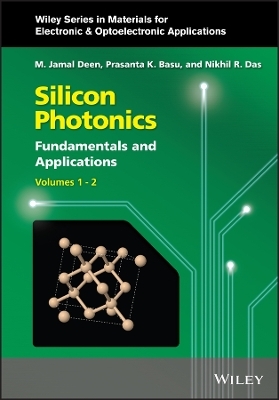
Silicon Photonics, 2 Volume Set
John Wiley & Sons Inc (Verlag)
978-1-119-60127-2 (ISBN)
- Noch nicht erschienen (ca. März 2026)
- Versandkostenfrei
- Auch auf Rechnung
- Artikel merken
Silicon Photonics discusses the physics, technology, and device operation of photonic devices using silicon, Group IV semiconductors, and their alloys. The book delivers an optimal combination of background information about photonic structures with description of up-to-date results and trends in silicon photonics. This Second Edition includes a new chapter on nonlinear silicon photonics as well as numerous updates to existing content.
Readers will find information on the role of silicon in photonics and its advantages and disadvantages as well as the properties of these alloys. Subsequent chapters in Silicon Photonics explore topics including:
Quantum structures, covering quantum wells, wires, and dots, superlattices, Si-based quantum structures, and effects of electric fields
Optical processes, covering absorption processes in semiconductors, intervalence band absorption, free-carrier absorption, and recombination and luminescence
Si light modulators, covering electrorefraction, thermo-optic effects, modulators, and optical and electrical structures
Raman lasers, covering Raman scattering, the Raman effect in silicon, the Raman gain coefficient, and continuous-wave Raman lasers
Principles of planar waveguide devices, covering directional couplers and distributed Bragg reflectors
Silicon Photonics is an excellent resource on the subject for materials scientists, applied physicists, electrical engineers, and postgraduate students working in Si photonics.
M. Jamal Deen, PhD, is Director of the Micro- & Nano Systems Lab and Research Chair in Information Technology at McMaster University, Canada. Prasanta Kumar Basu, PhD, worked in the Institute of Radio Physics and Electronics at the University of Calcutta, India, as a Lecturer, then as a Reader and a Professor, until his retirement. Nikhil R. Das, PhD, Professor at the University of Calcutta, India, specializes in semiconductor nanoelectronics and photonics.
1 Introduction to Silicon Photonics
1.1 Introduction
1.2 VLSI: Past, Present, and Future Roadmap
1.3 The Interconnect Problem in VLSI
1.4 The Long-Haul Optical Communication Link
1.5 Data Network
1.6 Conclusions
1.7 Scope of the Book
2 Basic Properties of Silicon
2.1 Introduction
2.2 Band Structure
2.3 Density-of-States Function
2.4 Impurities
2.5 Alloys of Silicon and Other Group IV Elements
2.6 Heterojunctions and Band Lineup
2.7 Si-Based Heterostructures
2.8 Direct GAP: Ge/SiGeSn Heterojunctions
3 Quantum Structures
3.1 Introduction
3.2 Quantum Wells
3.3 Quantum Wires and Dots
3.4 Superlattices
3.5 Si-Based Quantum Structures
3.6 Effect of Electric Field
4 Optical Processes
4.1 Introduction
4.2 Optical Constants
4.3 Basic Concepts
4.4 Absorption Processes in Semiconductors
4.5 Fundamental Absorption in Direct GAP
4.6 Fundamental Absorption in Indirect GAP
4.7 Absorption and Gain
4.8 Intervalence Band Absorption
4.9 Free-carrier Absorption
4.10 Recombination and Luminescence
4.11 Nonradiative Recombination
4.12 Excitonic and Impurity Absorption
5 Optical Processes in Quantum Structures
5.1 Introduction
5.2 Optical Processes in QWs
5.3 Intersubband Transitions
5.4 Excitonic Processes in QWs
5.5 Effect of Electric Fields
5.6 Optical Processes in QWRs
5.7 Optical Processes in QDS
6 Light Emitters in Si
6.1 Introduction
6.2 Basic Theory of Light Emission
6.3 Early Efforts: Zone Folding
6.4 Band Structure Engineering Using Alloys
6.5 Quantum Confinement
6.6 Impurities in Silicon
6.7 Stimulated Emission: Prospect
6.8 Intersubband Emission
6.9 Tensile-Strained Ge Layers
7 Si Light Modulators
7.1 Introduction
7.2 Physical Effects
7.3 Electrorefraction in Silicon
7.4 Thermo-Optic Effects in Si
7.5 Modulators: Some Useful Characteristics
7.6 Modulation Bandwidth under Injection
7.7 Optical Structures
7.8 Electrical Structures
7.9 High-Bandwidth Modulators
7.10 Performance of EO Modulators
8 Silicon Photodetectors
8.1 Introduction
8.2 Optical Detection
8.3 Important Characteristics of Photodetectors
8.4 Examples of Types of Photodetectors
8.5 Examples of Photodiodes in Standard Silicon Technology
8.6 Phototransistors in Standard Silicon Technology
8.7 CMOS and BiCMOS
8.8 Silicon-on-Insulator (SOI)
8.9 Photodetectors Using Heteroepitaxy
9 Raman Lasers
9.1 Introduction
9.2 Raman Scattering: Basic Concepts
9.3 Simplified Theory of Raman Scattering
9.4 Raman Effect in Silicon
9.5 Raman Gain Coefficient
9.6 Continuous-Wave Raman Laser
9.7 Further Developments
10 Guided Lightwaves: Introduction
10.1 Introduction
10.2 Ray Optic Theory for Light Guidance
10.3 Reflection Coefficients
10.4 Modes of a Planar Waveguide
10.5 Wave Theory of Light Guides
10.6 3D Optical Waveguides
10.7 Loss Mechanisms in Waveguides
10.8 Coupling to Optical Devices
10.9 Tapers
11 Principle of Planar Waveguide Devices
11.1 Introduction
11.2 Model for Mode Coupling
11.3 Directional Coupler
11.4 Distributed Bragg Reflector
11.5 Some Useful Planar Devices
12 Waveguides for Dense Wavelength-Division Multiplexing (DWDM) Systems
12.1 Introduction
12.2 Structure and Operation of AWGs
12.3 AWG Characteristics
12.4 Methods for Improving Performance
12.5 Applications of AWGs
12.6 PHASAR-Based Devices on Different Materials
12.7 Echelle Grating
13 Nonlinear Silicon Photonics
13.1 Introduction
13.2 Nonlinear Optical Effects in Silicon
13.3 Third-Order Nonlinearities
13.4 Two-Photon Absorption
13.5 Free-Carrier Effects
13.6 Nonlinear Waveguides
13.7 Nonlinear Resonators
13.8 Applications in Signal Processing
13.9 Future Directions
14 Fabrication Techniques and Materials Systems
14.1 Introduction
14.2 Planar Processing
14.3 Substrate Growth and Preparation
14.4 Material Modification
14.5 Etching
14.6 Lithography
14.7 Fabrication of Waveguides
14.8 Grating Formation Process
14.9 Materials Systems for Waveguide Formation
| Erscheint lt. Verlag | 12.3.2026 |
|---|---|
| Reihe/Serie | Wiley Series in Materials for Electronic & Optoelectronic Applications |
| Mitarbeit |
Herausgeber (Serie): Nikhil R. Das, Safa O. Kasap, Arthur Willoughby |
| Verlagsort | New York |
| Sprache | englisch |
| Maße | 170 x 244 mm |
| Themenwelt | Technik ► Maschinenbau |
| ISBN-10 | 1-119-60127-4 / 1119601274 |
| ISBN-13 | 978-1-119-60127-2 / 9781119601272 |
| Zustand | Neuware |
| Informationen gemäß Produktsicherheitsverordnung (GPSR) | |
| Haben Sie eine Frage zum Produkt? |
aus dem Bereich


