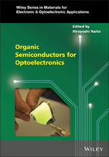
Organic Semiconductors for Optoelectronics (eBook)
John Wiley & Sons (Verlag)
978-1-119-14612-4 (ISBN)
Comprehensive coverage of organic electronics, including fundamental theory, basic properties, characterization methods, device physics, and future trends
Organic semiconductor materials have vast commercial potential for a wide range of applications, from self-emitting OLED displays and solid-state lighting to plastic electronics and organic solar cells. As research in organic optoelectronic devices continues to expand at an unprecedented rate, organic semiconductors are being applied to flexible displays, biosensors, and other cost-effective green devices in ways not possible with conventional inorganic semiconductors.
Organic Semiconductors for Optoelectronics is an up-to-date review of the both the fundamental theory and latest research and development advances in organic semiconductors. Featuring contributions from an international team of experts, this comprehensive volume covers basic properties of organic semiconductors, characterization techniques, device physics, and future trends in organic device development. Detailed chapters provide key information on the device physics of organic field-effect transistors, organic light-emitting diodes, organic solar cells, organic photosensors, and more. This authoritative resource:
- Provides a clear understanding of the optoelectronic properties of organic semiconductors and their influence to overall device performance
- Explains the theories behind relevant mechanisms in organic semiconducting materials and in organic devices
- Discusses current and future trends and challenges in the development of organic optoelectronic devices
- Reviews electronic properties, device mechanisms, and characterization techniques of organic semiconducting materials
- Covers theoretical concepts of optical properties of organic semiconductors including fluorescent, phosphorescent, and thermally-assisted delayed fluorescent emitters
An important new addition to the Wiley Series in Materials for Electronic & Optoelectronic Applications, Organic Semiconductors for Optoelectronics bridges the gap between advanced books and undergraduate textbooks on semiconductor physics and solid-state physics. It is essential reading for academic researchers, graduate students, and industry professionals involved in organic electronics, materials science, thin film devices, and optoelectronics research and development.
Edited by
Hiroyoshi Naito, Professor in the Department of Physics and Electronics at Osaka Prefecture University, Japan, where he has taught for over 30 years. He has authored and co-authored more than 300 journal publications, contributed several book chapters, and has attended numerous conferences as an invited speaker. His research is focused on the characterization of optical and electronic properties of organic semiconductors and the device physics of organic optoelectronic devices.
Series Editors
Arthur Willoughby University of Southampton, Southampton, UK
Peter Capper Ex-Leonardo MW Ltd, Southampton, UK
Safa Kasap University of Saskatchewan, Saskatoon, Canada
Comprehensive coverage of organic electronics, including fundamental theory, basic properties, characterization methods, device physics, and future trends Organic semiconductor materials have vast commercial potential for a wide range of applications, from self-emitting OLED displays and solid-state lighting to plastic electronics and organic solar cells. As research in organic optoelectronic devices continues to expand at an unprecedented rate, organic semiconductors are being applied to flexible displays, biosensors, and other cost-effective green devices in ways not possible with conventional inorganic semiconductors. Organic Semiconductors for Optoelectronics is an up-to-date review of the both the fundamental theory and latest research and development advances in organic semiconductors. Featuring contributions from an international team of experts, this comprehensive volume covers basic properties of organic semiconductors, characterization techniques, device physics, and future trends in organic device development. Detailed chapters provide key information on the device physics of organic field-effect transistors, organic light-emitting diodes, organic solar cells, organic photosensors, and more. This authoritative resource: Provides a clear understanding of the optoelectronic properties of organic semiconductors and their influence to overall device performance Explains the theories behind relevant mechanisms in organic semiconducting materials and in organic devices Discusses current and future trends and challenges in the development of organic optoelectronic devices Reviews electronic properties, device mechanisms, and characterization techniques of organic semiconducting materials Covers theoretical concepts of optical properties of organic semiconductors including fluorescent, phosphorescent, and thermally-assisted delayed fluorescent emitters An important new addition to the Wiley Series in Materials for Electronic & Optoelectronic Applications, Organic Semiconductors for Optoelectronics bridges the gap between advanced books and undergraduate textbooks on semiconductor physics and solid-state physics. It is essential reading for academic researchers, graduate students, and industry professionals involved in organic electronics, materials science, thin film devices, and optoelectronics research and development.
Hiroyoshi Naito, Professor in the Department of Physics and Electronics at Osaka Prefecture University, Japan, where he has taught for over 30 years. He has authored and co-authored more than 300 journal publications, contributed several book chapters, and has attended numerous conferences as an invited speaker. His research is focused on the characterization of optical and electronic properties of organic semiconductors and the device physics of organic optoelectronic devices. Series Editors Arthur Willoughby University of Southampton, Southampton, UK. Peter Capper Ex?]Leonardo MW Ltd, Southampton, UK. Safa Kasap University of Saskatchewan, Saskatoon, Canada.
Preface - to be supplied by H.Naito
1 Electronic Structures of Organic Semiconductors
Kazuyoshi Tanaka
2 Charge carrier transport
Hiroyoshi Naito
3 Theory of Optical Properties of Organic Semiconductors
Jai Singh, Monishka Rita Narayan and David Ompong
4 Light absorption and emission properties of organic semiconductors
Takashi Kobayashi, Takashi Nagase, and Hiroyoshi Naito
5 Photoluminescence Spectroscopy
Hiroyoshi Naito
6 Time-of-flight method for determining the drift mobility in organic semiconductors
Masahiro Funahashi
7 Microwave and Terahertz Spectroscopy
Akinori Saeki
8 Intrinsic and extrinsic transport in crystalline organic semiconductors: electron-spin-resonance study for characterization of localized states.
A. S. Mishchenko
9 Second Harmonic Generation Spectroscopy
Takaaki Manaka and Mitsumasa Iwamoto
10 Device Physics of organic field-effect transistors
Hiroyuki Matsui
11 Spontaneous orientation polarization in organic light-emitting diodes and its inuence on charge injection, accumulation, and degradation properties
Yutaka Noguchi, Hisao Ishii, Lars Jäger, Tobias D. Schmidt, Wolfgang Brütting
12 Advanced molecular design for organic light emitting diode emitters based on horizontal molecular orientation and thermally activated delayed fluorescence
Li Zhao, DaeHyeon Kim, Jean-Charles Ribierre, Takeshi Komino and Chihaya Adachi
13 Organic field effect transistors integrated circuits
Mayumi Uno
14 Naphthobisthiadiazole-based semiconducting polymers for high-efficiency organic photovoltaics
Itaru Osaka and Kazuo Takimiya
15 Plasmonics for light-emitting and photovoltaic devices
Koichi Okamoto
1
Electronic Structures of Organic Semiconductors
Kazuyoshi Tanaka
Fukui Institute for Fundamental Chemistry, Kyoto University, Kyoto, Japan
CHAPTER MENU
- Introduction
- Electronic Structures of Organic Crystalline Materials
- Injection of Charge Carriers
- Transition from the Conductive State
- Electronic Structure of Organic Amorphous Solid
- Conclusion
1.1 Introduction
Electric conductivities of organic materials are normally low and they are classified as insulators or semiconductors. In general, electric conductivity of the semiconductor is broadly considered to be in the range from 10−10 to 102 Scm−1 (Figure 1.1). Electric conductivity σ is expressed by
where n is the number of charge carriers for electric transport, e the elementary charge ( C), and μ the mobility of the carriers. Appearance of high conductivity in organic material per se is quite rare or completely absent. This is because organic materials do not have enough number of n though they might have large μ in a potential sense embodied by, e. g., extended π‐conjugation appropriate to the electric conduction throughout the material.
The above description means that organic materials can change into semiconductive or even metallic state in terms of appropriate injection of carriers if they are guaranteed to show appropriate μ values. From the latter half of the previous century, a great deal of attempts toward this direction have been piled up and nowadays organic semiconductors or organic metals have become quite common members in electronics materials such as organic field‐effect transistor (OFET), organic light‐emitting diode (OLED), organic photovoltaic (OPV) device, and so on. It is noted here that characteristic features of organic semiconductors or organic metals come from their structural low dimensionality. This is simultaneously accompanied with the fact that the direction of electric transport is remarkably developed toward one or two directions in the material and, in this sense, these are called one‐dimensional (1D) or two‐dimensional (2D) materials. For example, polymer with rather rigid spine can be regarded as 1D material and graphene a complete 2D material. These low‐dimensional materials often show peculiar behavior in relation to electronic properties when they are in the semiconductive or metallic state.
Figure 1.1 Logarithmic representation of electric conductivity σ (S/cm) of miscellaneous materials at room temperature.
Analysis of the electronic structure is of primary importance in consideration of the semiconductive or metallic properties of organic materials. In this Chapter, we are to study (i) the ways of carrier injections and (ii) transition from the conductive state inherent in low‐dimensional materials, with respect to organic semiconductors. Emphasis will also be put on understanding of the electronic properties of these materials based on their electronic structures. We first start from the electronic structures of organic materials with regular repetition of molecular unit, that is, crystalline structure, and then elucidate the electronic properties derived from the electronic structures. The prospects for typical conductive polymers and charge‐transfer organic crystals are also to be afforded. In the last part, the electronic properties of organic amorphous material will also be dealt with.
1.2 Electronic Structures of Organic Crystalline Materials
In this Section, electronic structure and its related quantities of organic materials with crystalline structures are described with respect to the 1D system not only for the sake of simplicity but also due to being realistic in most of the organic semiconductors. Note that the 1D organic crystal has regular repetition of the unit cells as illustrated in Figure 1.2 being somewhat similar to the primary structure of ideal polymers. Extension to 2D or 3D crystal is quite straightforward. In order to describe the electronic structure of organic crystal, the orbital approximation occurring from one‐electron picture is to be employed throughout this Section unless specially noted, since it allows us to have a simple but clear idea in the same spirit as the molecular orbital (MO) scheme for the ordinary organic molecules. In organic crystals, the wavefunction based on the one‐electron picture is often mentioned as crystal orbital (CO) as is described later. We will try to figure out the electronic properties of organic crystals mainly derived from the COs.
Figure 1.2 Schematic drawing of 1D crystal.
1.2.1 Free‐Electron Picture
First, we start from the simplest wavefunction of a free electron in 1D space, using the Schrödinger equation which is expressed as
without any potentials for a free electron. The wavefunction of a free electron at a point x is accompanied with a variable k as
where i stands for the imaginary unit and k is called wavevector (or wave number) being proportional to momentum p of the electron, that is,
with , h being the Planck's constant. As a matter of course, k becomes vector k for 2D and 3D cases. Furthermore, A and B in Eq. (1.3) are the formal normalization constants. Each of the two terms in the right‐hand side of Eq. (1.3) signifies the motion of a free electron to the x and –x directions.
The free‐electron wavefunction basically describes the electron motion in a free space without any potentials as is mentioned above and, in this sense, is considered to describe the electrons inside the space of crystal as ideal gas. Note this wavefunction takes a complex value, which is natural in the picture of quantum mechanics. The energy of a free electron is a function of k and is given by
which has a continuous parabolic shape with a variable k as shown in Figure 1.3. The plot of the energy value depending on k is generally called energy band or band structure. According to the number of electrons, there appears the upper limit of energy levels filled with electrons called Fermi energy (ɛF) dividing both the valence and conduction bands. The wavevector at the position of ɛF is called Fermi wavevector kF. Note that ±k gives the same energy signifying the degeneracy according to inversion of the momentum, which is also mentioned as time‐reversal symmetry due to the change of momentum direction.
Figure 1.3 Energy band of a free electron. ɛF and kF signify Fermi energy and Fermi wave vector, respectively.
1.2.2 Tight‐Binding Framework
1.2.2.1 Formalism
The next step is to introduce an infinite array of the unit cells in the concerning organic 1D crystal structure already shown in Figure 1.2. This concept simultaneously brings about the spatial regular array of potentials V(x) in Figure 1.4 into the Schrödinger equation as
Figure 1.4 Model potential of 1D crystal.
where
with a being the translation length. Several examples of unit cells in the organic 1D and 2D crystals are given in Figure 1.5.
Figure 1.5 Examples of 1D (a), (b) and 2D (c), (d) crystals and the unit cells (shown in parentheses, oval, or square). The arrows indicate the direction(s) of the translation.
In order to obtain the plausible wavefunction for general 1D crystal with infinite repetition of the unit cells shown in Figure 1.2, periodic boundary condition (or Born‐von Karman boundary condition) is introduced toward simple mathematical treatment as in the ordinary solid‐state physics. This condition is embodied by considering a huge “ring” with an infinite diameter consisting of an infinite array of the unit cells as shown in Figure 1.6. This makes the 1D free‐electron wavefunction in Eq. (1.3) change into the 1D Bloch function which satisfies the relationship
Figure 1.6 Periodic boundary condition expressed by a ring with an infinitely large diameter. The first unit cell (black circle) becomes overlapped with the last unit cell after the infinite translation.
where, again, k signifies the wavevector and a the translation length. The Bloch function is considered as deformation of the free‐electron wavefunction into that modulated by the array of the unit cells containing the atoms or molecules. Also note that Eq. (1.8) signifies that the translated wavefunction ψ(x + a) is represented by multiplication of the phase factor exp[ika] to the original function ψ(x). The value of k ranges from –π/a to π/a, which is...
| Erscheint lt. Verlag | 30.7.2021 |
|---|---|
| Reihe/Serie | Wiley Series in Materials for Electronic & Optoelectronic Applications | Wiley Series in Materials for Electronic & Optoelectronic Applications |
| Sprache | englisch |
| Themenwelt | Naturwissenschaften ► Chemie |
| Technik ► Elektrotechnik / Energietechnik | |
| Technik ► Maschinenbau | |
| Schlagworte | Electrical & Electronics Engineering • Electronic materials • Elektronische Materialien • Elektrotechnik u. Elektronik • Halbleiterphysik • Materials Science • Materialwissenschaften • optoelectronic device physics • Optoelektronik • organic device development • Organic electronics • organic optoelectronics • Organic semiconductors • organic semiconductors characterization • organic semiconductors properties • organic semiconductors spectroscopy • organic semiconductor theory • Organische Elektronik • Organischer Halbleiter • Physics • Physik • Semiconductor physics |
| ISBN-10 | 1-119-14612-7 / 1119146127 |
| ISBN-13 | 978-1-119-14612-4 / 9781119146124 |
| Informationen gemäß Produktsicherheitsverordnung (GPSR) | |
| Haben Sie eine Frage zum Produkt? |
Kopierschutz: Adobe-DRM
Adobe-DRM ist ein Kopierschutz, der das eBook vor Mißbrauch schützen soll. Dabei wird das eBook bereits beim Download auf Ihre persönliche Adobe-ID autorisiert. Lesen können Sie das eBook dann nur auf den Geräten, welche ebenfalls auf Ihre Adobe-ID registriert sind.
Details zum Adobe-DRM
Dateiformat: EPUB (Electronic Publication)
EPUB ist ein offener Standard für eBooks und eignet sich besonders zur Darstellung von Belletristik und Sachbüchern. Der Fließtext wird dynamisch an die Display- und Schriftgröße angepasst. Auch für mobile Lesegeräte ist EPUB daher gut geeignet.
Systemvoraussetzungen:
PC/Mac: Mit einem PC oder Mac können Sie dieses eBook lesen. Sie benötigen eine
eReader: Dieses eBook kann mit (fast) allen eBook-Readern gelesen werden. Mit dem amazon-Kindle ist es aber nicht kompatibel.
Smartphone/Tablet: Egal ob Apple oder Android, dieses eBook können Sie lesen. Sie benötigen eine
Geräteliste und zusätzliche Hinweise
Buying eBooks from abroad
For tax law reasons we can sell eBooks just within Germany and Switzerland. Regrettably we cannot fulfill eBook-orders from other countries.
aus dem Bereich


