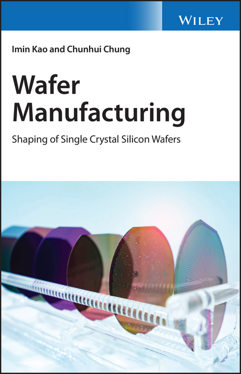
Wafer Manufacturing (eBook)
John Wiley & Sons (Verlag)
978-1-118-69623-1 (ISBN)
Presenting all the major stages in wafer manufacturing, from crystals to prime wafers.
This book first outlines the physics, associated metrology, process modelling and quality requirements and the goes on to discuss wafer forming and wafer surface preparation techniques. The whole is rounded off with a chapter on the research and future challenges in wafer manufacturing.
Imin Kao, is Professor in the Department of Mechanical Engineering at the State University of New York in Stony Brook, USA. He is Faculty Director of the Undergraduate College in Information and Technology Studies. He holds three patents, and his research foci include robotic manipulation with soft contacts and smart contact surface technology using MEMS.
Chunhui Chung, is Associate Professor in the Department of Mechanical Engineering at the National Cheng Kung University in Taiwan.
Presenting all the major stages in wafer manufacturing, from crystals to prime wafers. This book first outlines the physics, associated metrology, process modelling and quality requirements and the goes on to discuss wafer forming and wafer surface preparation techniques. The whole is rounded off with a chapter on the research and future challenges in wafer manufacturing.
Imin Kao, is Professor in the Department of Mechanical Engineering at the State University of New York in Stony Brook, USA. He is Faculty Director of the Undergraduate College in Information and Technology Studies. He holds three patents, and his research foci include robotic manipulation with soft contacts and smart contact surface technology using MEMS. Chunhui Chung, is Associate Professor in the Department of Mechanical Engineering at the National Cheng Kung University in Taiwan.
1
Wafers and Semiconductors
1.1 Introduction
The fundamental building block from which microelectronic integrated circuit (IC) chips, MEMS (micro electro mechanical systems) devices, and microelectronic devices and systems are constructed is called a “wafer.” This book discusses the nuances of the wafer manufacturing (or wafer production) technology and process, as well as the recent research and development contributing to the growth of the technologies in wafer manufacturing. Each chapter has a References section at the end to provide a list of books and articles for reference and further reading or study on the subjects presented.
This chapter provides basic information about wafers and the semiconductor revolution that has influenced our modern daily lives, including the subjects of silicon, wafers, mechanical materials, and surface properties.
1.2 Semiconductor Revolution
1.2.1 Classification of Materials
Materials are classified, based on their electrical conductivity, into the following four categories: conductor, insulator, superconductor, and semiconductor. Table 1.1 lists a few selected materials in the three most common categories and their resistivity values in m. The resistance of a material, is defined as follows
where is the resistivity and and are the length and cross‐sectional area of the material, respectively. When a voltage is applied to a material, it may cause electrical current to flow, depending on the resistivity of the material. The electrical resistivity is thus defined as the ratio between the electric field and the density of the current it creates, as in the following equation
where is the electric field applied inside the material with a unit of V , and is the current density in A m, also measured inside the material. The conductivity is the inverse of resistivity as follows
Four classifications of material are described in the following.
- Conductor – these materials conduct current when a voltage is applied. Examples include metals, many metal alloys, and carbon. Metals are the best naturally occurring conductors of electricity, because of their metallic bonding, and thus have low resistivity (see Table 1.1).
- Insulator – these materials conduct no current when a voltage is applied. Nevertheless, the current will suddenly pass through the material if the voltage is high enough, for example, in the form of an arc or plasma. An insulator is sometimes referred to as a dielectric, which describes non‐conduction of a direct current. The dielectric strength of an insulating material, then, is the electrical potential required to break down the insulator per unit thickness, with typical unit in V (or V ). Examples of insulator materials include silicon dioxide (), glass, ceramic materials, polymers, etc. Most ceramics and polymers, whose electrons are tightly bound by covalent and/or ionic bonding, are typically poor conductors. Many of these materials are used as insulators because they possess high resistivity values (See Table 1.1).
- Superconductor – a superconductor is a material that exhibits zero resistivity. Superconductivity is a phenomenon that is observed in certain materials at low temperatures near absolute zero at which zero electrical resistance and expulsion of magnetic fields take place in certain materials. Such materials hold great interest and promise for many applications such as power transmission, magnetic levitation, and electronic switching.
- Semiconductor – a semiconductor is dielectric in its natural state, but can conduct electricity under some conditions, either due to the addition of an impurity or because of temperature effects, but not others. Such characteristics make semiconductor materials a good medium for the control of electrical current. The resistivity of a semiconductor lies between that of insulators and conductors. Typical resistivities of semiconductor materials range from 10 to m. Semiconductors are the foundation of modern electronics, including computers, electronic devices, and smart phones. Semiconductor solar photovoltaic panels directly convert light energy into electricity.
Table 1.1 Resistivity of selected materials in m, as defined in Equation (1.1). Superconductors have zero resistivity.
Values of resistivity vary depending on condition and environment, such as impurity and temperature. The commonly used unit in semiconductors is cm, with 1 m = 100 cm.
Conductors Resistivity Insulators Resistivity Semiconductors Resistivity Aluminum Polyurethane Silicon Silver Rubber – Germanium Copper – GaAs – Carbon Glass – SiC – Common semiconducting materials are crystalline solids. Silicon is the most popular commercial semiconductor material. Many other materials are used, including germanium, gallium arsenide (GaAs), indium phosphide (InP), and silicon carbide (SiC). The electronic properties and the conductivity of a semiconductor can be changed by “doping,” referring to a diffusion process that adds other materials to the semiconductor materials. This is typically achieved during crystalline silicon growth by adding boron or phosphorus impurities to the melt and then allowing it to solidify into silicon during the crystal growth process.
1.2.2 Semiconductor Revolution Today
Presently we are in the midst of a “semiconductor revolution.” Many objects with which we are associated today have either semiconductor devices built in or have been manufactured with a machine that contains in‐built semiconductor devices. These modern times are the “semiconductor era”, akin to the “steel era” that propelled the “second industrial revolution” in the 19th century. In the last several decades, semiconductor technology has grow in leaps and bounds, partly driven by consumerism generated by telecommunication, wireless internet, and information technology and partly by the need for automation catering to mass or batch production and manufacturing of technologically sophisticated products. Thanks to semiconductor technology, we are now able to manufacture very complex products in large quantities at lower costs.
Today's world is embraced by three technologies, each in a different stage of maturity:
- The microelectronics technology with integrated circuits (ICs) has been at the forefront of all the breath‐taking achievements realized in the past few decades. At the core of IC technology is the development of very tiny but extremely robust electrical circuits that can act as the brain of a machine, such as that in a controller, computer, or smart devices. The road of microelectronics technology was paved with the invention of the first transistor in 1947 [American Physical Society (2000); Riordan and Hoddeson (1997)], as shown in Figure 1.1. The batch fabrication of transistors using planar technology enables the IC technology we know today. IC technology has been growing rapidly since the 1970s and since that time it has never shown any sign of decline. Radically new technologies and new products are still being introduced into the market every year and new concepts and innovations are being researched that will keep this technology moving for years to come.
- The fabrication technology of IC has given birth to the world of MEMS (micro electro mechanical systems) which integrates the electrical power of ICs with micron‐scale mechanical structures to build powerful applications pertaining to the real world. An example is air‐bag sensors in automobiles. MEMS technology is in an exciting phase; it has already been utilized in everyday applications and is still concurrently looking for new applications. The “satellite navigation” industry and the “computer gaming industry” have already presented some new avenues, and there are undoubtedly many more opportunities to realize.
Figure 1.1 The first transistor, made of germanium, at the AT&T Bell Laboratory.
(Source: AT&T)
- On the horizon is the new enticing world of “nanotechnology”, which encompasses both fundamental research and promising applications in fields such as medicine, energy, biomedical, etc. At the root of nanotechnology is the confluence of electrical, mechanical, chemical, physical, and biological sciences and engineering. The fields of nanotechnology hold a lot of future promise.
The most fundamental part of the semiconductor world is the “semiconductor material” used to realize the technologies. In layman's parlance, semiconductors can show electrical conductivity between conductors and insulators, as described in Section 1.2.1. This property by itself is not enough to realize the technologies (ICs and MEMS) we know of today. What really drives today's semiconductor world are the properties of some of the...
| Erscheint lt. Verlag | 5.1.2021 |
|---|---|
| Sprache | englisch |
| Themenwelt | Naturwissenschaften ► Chemie |
| Technik ► Elektrotechnik / Energietechnik | |
| Technik ► Maschinenbau | |
| Schlagworte | Electrical & Electronics Engineering • Electronic materials • Elektronische Materialien • Elektrotechnik u. Elektronik • Halbleiter • Halbleiterphysik • materials processing • Materials Science • Materialverarbeitung • Materialwissenschaften • Physics • Physik • Semiconductor physics • Wafer |
| ISBN-10 | 1-118-69623-9 / 1118696239 |
| ISBN-13 | 978-1-118-69623-1 / 9781118696231 |
| Informationen gemäß Produktsicherheitsverordnung (GPSR) | |
| Haben Sie eine Frage zum Produkt? |
Kopierschutz: Adobe-DRM
Adobe-DRM ist ein Kopierschutz, der das eBook vor Mißbrauch schützen soll. Dabei wird das eBook bereits beim Download auf Ihre persönliche Adobe-ID autorisiert. Lesen können Sie das eBook dann nur auf den Geräten, welche ebenfalls auf Ihre Adobe-ID registriert sind.
Details zum Adobe-DRM
Dateiformat: EPUB (Electronic Publication)
EPUB ist ein offener Standard für eBooks und eignet sich besonders zur Darstellung von Belletristik und Sachbüchern. Der Fließtext wird dynamisch an die Display- und Schriftgröße angepasst. Auch für mobile Lesegeräte ist EPUB daher gut geeignet.
Systemvoraussetzungen:
PC/Mac: Mit einem PC oder Mac können Sie dieses eBook lesen. Sie benötigen eine
eReader: Dieses eBook kann mit (fast) allen eBook-Readern gelesen werden. Mit dem amazon-Kindle ist es aber nicht kompatibel.
Smartphone/Tablet: Egal ob Apple oder Android, dieses eBook können Sie lesen. Sie benötigen eine
Geräteliste und zusätzliche Hinweise
Buying eBooks from abroad
For tax law reasons we can sell eBooks just within Germany and Switzerland. Regrettably we cannot fulfill eBook-orders from other countries.
aus dem Bereich


