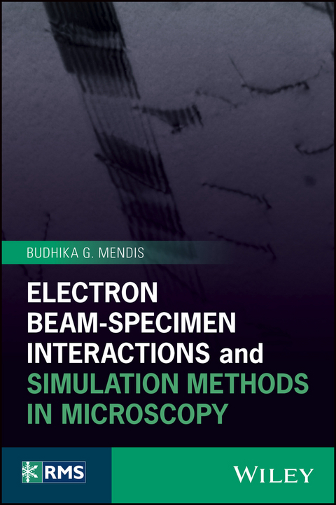
Electron Beam-Specimen Interactions and Simulation Methods in Microscopy (eBook)
John Wiley & Sons (Verlag)
978-1-118-69665-1 (ISBN)
A detailed presentation of the physics of electron beam-specimen interactions
Electron microscopy is one of the most widely used characterisation techniques in materials science, physics, chemistry, and the life sciences. This book examines the interactions between the electron beam and the specimen, the fundamental starting point for all electron microscopy. Detailed explanations are provided to help reinforce understanding, and new topics at the forefront of current research are presented. It provides readers with a deeper knowledge of the subject, particularly if they intend to simulate electron beam-specimen interactions as part of their research projects. The book covers the vast majority of commonly used electron microscopy techniques. Some of the more advanced topics (annular bright field and dopant atom imaging, atomic resolution chemical analysis, band gap measurements) provide additional value, especially for readers who have access to advanced instrumentation, such as aberration-corrected and monochromated microscopes.
Electron Beam-Specimen Interactions and Simulation Methods in Microscopy offers enlightening coverage of: the Monte-Carlo Method; Multislice Simulations; Bloch Waves in Conventional and Analytical Transmission Electron Microscopy; Bloch Waves in Scanning Transmission Electron Microscopy; Low Energy Loss and Core Loss EELS. It also supplements each chapter with clear diagrams and provides appendices at the end of the book to assist with the pre-requisites.
- A detailed presentation of the physics of electron beam-specimen interactions
- Each chapter first discusses the background physics before moving onto simulation methods
- Uses computer programs to simulate electron beam-specimen interactions (presented in the form of case studies)
- Includes hot topics brought to light due to advances in instrumentation (particularly aberration-corrected and monochromated microscopes)
Electron Beam-Specimen Interactions and Simulation Methods in Microscopy benefits students undertaking higher education degrees, practicing electron microscopists who wish to learn more about their subject, and researchers who wish to obtain a deeper understanding of the subject matter for their own work.
BUDHIKA G. MENDIS, PhD, is Associate Professor at the Department of Physics, Durham University, UK, where he teaches electron microscopy at both undergraduate and postgraduate levels. He has over 15 years of experience in all the major electron microscopy techniques, including aberration-correction, and has used many of the simulation methods discussed in this book as part of his own research.
A detailed presentation of the physics of electron beam-specimen interactions Electron microscopy is one of the most widely used characterisation techniques in materials science, physics, chemistry, and the life sciences. This book examines the interactions between the electron beam and the specimen, the fundamental starting point for all electron microscopy. Detailed explanations are provided to help reinforce understanding, and new topics at the forefront of current research are presented. It provides readers with a deeper knowledge of the subject, particularly if they intend to simulate electron beam-specimen interactions as part of their research projects. The book covers the vast majority of commonly used electron microscopy techniques. Some of the more advanced topics (annular bright field and dopant atom imaging, atomic resolution chemical analysis, band gap measurements) provide additional value, especially for readers who have access to advanced instrumentation, such as aberration-corrected and monochromated microscopes. Electron Beam-Specimen Interactions and Simulation Methods in Microscopy offers enlightening coverage of: the Monte-Carlo Method; Multislice Simulations; Bloch Waves in Conventional and Analytical Transmission Electron Microscopy; Bloch Waves in Scanning Transmission Electron Microscopy; Low Energy Loss and Core Loss EELS. It also supplements each chapter with clear diagrams and provides appendices at the end of the book to assist with the pre-requisites. A detailed presentation of the physics of electron beam-specimen interactions Each chapter first discusses the background physics before moving onto simulation methods Uses computer programs to simulate electron beam-specimen interactions (presented in the form of case studies) Includes hot topics brought to light due to advances in instrumentation (particularly aberration-corrected and monochromated microscopes) Electron Beam-Specimen Interactions and Simulation Methods in Microscopy benefits students undertaking higher education degrees, practicing electron microscopists who wish to learn more about their subject, and researchers who wish to obtain a deeper understanding of the subject matter for their own work.
BUDHIKA G. MENDIS, PhD, is Associate Professor at the Department of Physics, Durham University, UK, where he teaches electron microscopy at both undergraduate and postgraduate levels. He has over 15 years of experience in all the major electron microscopy techniques, including aberration-correction, and has used many of the simulation methods discussed in this book as part of his own research.
Preface ix
1 Introduction 1
1.1 Organisation and Scope of the Book 3
References 8
2 The Monte Carlo Method 9
2.1 Physical Background and Implementation 11
2.1.1 Elastic Scattering By an Atomic Nucleus 11
2.1.2 Inelastic Scattering by Atomic Electrons 18
2.1.3 Implementation of the Monte Carlo Algorithm 23
2.2 Some Applications of the Monte Carlo Method 27
2.2.1 Spatial Resolution and Backscattered Imaging 27
2.2.2 Characteristic X-Ray Generation 34
2.2.3 Cathodoluminescence and Electron Beam Induced Current Microscopy 37
2.3 Further Topics in Monte Carlo Simulations 40
2.3.1 Classical or Quantum Physics? 40
2.3.2 Spin-Orbit Coupling and the Mott Cross-Section 43
2.3.3 Dielectric Model of Stopping Power and Secondary Electron Emission 46
2.4 Summary 49
References 50
3 Multislice Method 53
3.1 Mathematical Treatment of the Multislice Method 56
3.1.1 Specimen Transmission Function 59
3.1.2 Fresnel Propagator Function 66
3.1.3 Objective Lens Contrast Transfer Function and Partial Coherence 71
3.1.4 Implementation of the Multislice Algorithm 76
3.2 Applications of Multislice Simulations 78
3.2.1 HREM Imaging and Electron Crystallography 78
3.2.2 CBED and STEM Applications: Frozen Phonon Model 87
3.3 Further Topics in Multislice Simulation 93
3.3.1 Accuracy of Multislice Algorithms 93
3.3.2 Is the Frozen Phonon Model Physically Realistic? 97
3.4 Summary 102
References 102
4 Bloch Waves 105
4.1 Basic Principles 106
4.1.1 Mathematical Background 106
4.1.2 Application to Two-Beam Theory 111
4.1.3 Phenomenological Modelling of Thermal Diffuse Scattering 116
4.1.4 Bloch States in Zone-Axis Orientations 124
4.2 Applications of Bloch Wave Theory 132
4.2.1 HREM Imaging 132
4.2.2 HAADF Imaging 134
4.2.3 Bloch Wave Scattering By Elastic Strain Fields 144
4.3 Further Topics in Bloch Waves 149
4.3.1 Dopant Atom Imaging in STEM 149
4.3.2 Electron Channelling and Its Uses 156
4.4 Summary 160
References 161
5 Single Electron Inelastic Scattering 165
5.1 Fundamentals of Inelastic Scattering 166
5.1.1 Electron Excitation in a Single Atom by a Plane Wave 166
5.1.2 Mixed Dynamic Form Factor 180
5.1.3 Yoshioka Equations and Inelastic Scattering within a Crystal 189
5.1.4 Coherence in Inelastic Scattering 195
5.2 Fine Structure of The Electron Energy Loss Signal 201
5.2.1 Origin of Fine Structure 201
5.2.2 Core Hole Effects 206
5.2.3 Magnetic Circular Dichroism 209
5.3 Summary 211
References 212
6 Electrodynamic Theory of Inelastic Scattering 215
6.1 Bulk and Surface Energy Loss 216
6.1.1 Energy Loss in an 'Infinite' Solid 216
6.1.2 Phonon Spectroscopy 226
6.1.3 Interface and Surface Contributions 232
6.2 Radiative Phenomena 244
6.2.1 Cerenkov Radiation and Band Gap Measurement 244
6.2.2 Transition Radiation 249
6.3 Simulating Low Energy Loss EELS Spectra 253
6.3.1 Discrete Dipole Approximation (DDA) 253
6.3.2 Boundary Element Method (BEM) 254
6.4 Summary 259
References 259
Appendix A The First Born Approximation and Atom Scattering Factor 263
Appendix B Potential for an 'Infinite' Perfect Crystal 267
Appendix C The Transition Matrix Element in the One Electron Approximation 269
Appendix D Bulk Energy Loss in the Retarded Regime 271
Index 275
Introduction
Electron beam scattering has had a long and distinguished history. Some of the essential physics was investigated even before the first electron microscope was built. The unsuspecting reader may find it surprising to come across familiar names such as Bethe, Bohr, Rutherford, Fermi and Mott in this book. While electron beam scattering is a mature theory its widespread use in electron microscopy measurements is arguably a more recent phenomenon. This is primarily due to two reasons. The first is the processing speed of modern computers; even a standard desktop computer can now produce useful results within a reasonable time and thankfully there are many software packages that take advantage of this. The second reason is the emergence of a new generation of electron microscopes that can resolve atom columns that are less than an angstrom apart, that have ∼10 meV energy resolution or less for measuring vibronic modes and that can record events separated in time by femtoseconds. With such a wealth of new information there is a strong emphasis on extracting quantitative information about the sample. Electron beam scattering calculations are often indispensable for correct data interpretation.
Two examples help illustrate the advantages of combining experimental results with simulation. The first is using high angle annular dark field (HAADF) imaging in a scanning transmission electron microscope (STEM) to characterise the interface in an AlAs–GaAs superlattice (Robb and Craven, 2008; Robb et al., 2012). Figure 1.1a shows the HAADF image of a [110]-oriented, epitaxial AlAs–GaAs superlattice acquired using an aberration corrected STEM. In this orientation the Group III–V elements are distributed as closely spaced (i.e. ∼1.4 Å) atom column pairs or ‘dumbbells’. The HAADF signal increases monotonically with the atomic number of the scattering element, so that using AlAs dumbbells as an example, the intensity of an As column is larger than that of Al. Figure 1.1b is a histogram of the background subtracted column intensity ratio values for all dumbbells in Figure 1.1a. The two prominent peaks are due to dumbbells in ‘bulk’ AlAs and ‘bulk’ GaAs respectively. However, there are also intermediate values for the column intensity ratio (arrowed region in Figure 1.1b) and further analysis reveals these to be due to dumbbells located at the AlAs–GaAs interface region (Robb and Craven, 2008). An interface ‘width’ can be defined based on the 5–95% variation in column intensity ratio across the interface. The interface width is found to be independent of the specimen thickness for superlattices grown on an AlAs substrate, but not on GaAs substrate.
Figure 1.1 (a) HAADF STEM image of a [110]-oriented, AlAs–GaAs superlattice. The background subtracted column intensity ratio values for all dumbbells in (a) are shown in (b) as a histogram. (c) plots experimental and multislice simulated values for the AlAs–GaAs interface width, as defined from the column intensity ratio profile, as a function of specimen thickness. Supercells for the multislice simulation are constructed assuming a linear diffusion model and a more accurate diffusion model (Moison et al., 1989) valid for the AlAs–GaAs system. Results are shown for superlattices grown on GaAs (labelled ‘AlAs-on-GaAs’) and AlAs (labelled ‘GaAs-on-AlAs’) substrates respectively. (a) and (b)
From Robb and Craven (2008). Reproduced with permission; copyright Elsevier. (c) From Robb et al. (2012). Reproduced with permission; copyright Elsevier.
It is not clear if the interface width is due to chemical inter-diffusion, electron beam spreading within the sample or interfacial roughness. This can, however, be tested by constructing supercells representing the different scenarios and performing multislice simulations (Chapter 3). Figure 1.1c shows the simulated results for chemical diffusion. The interface width, as deduced from the column intensity ratio values, is plotted as a function of specimen thickness for a linear composition profile and a more realistic diffusion model valid for the AlAs–GaAs system (Moison et al., 1989). The latter accurately reproduces the experimental results, suggesting diffusion as a likely candidate. In fact, simulations for a saw tooth-shaped and smooth interface did not agree with experiment, so that interfacial roughness and beam spreading have only a secondary effect on the measurement (Robb et al., 2012).
The second example is the use of electron energy loss spectroscopy (EELS) to extract the local electronic density of states for a silicon dopant atom in graphene (Ramasse et al., 2013). As illustrated in Figure 1.2a, the silicon atom can be incorporated either through direct substitution (i.e. threefold coordination) or as a fourfold coordinated atom in defect regions of the graphene sheet. The dopant atom can be readily identified using HAADF imaging in an aberration corrected STEM, taking advantage of the higher atomic number of silicon compared to carbon. The solid lines in Figure 1.2b are the Si L2,3-EELS edges measured from the two different dopant atom configurations. Owing to the nature of inelastic scattering (Chapter 5) the shape of the EELS spectrum is governed by the angular momentum resolved unoccupied density of electronic states. The filled spectra in Figure 1.2b are the results obtained from density functional theory simulation. There is excellent agreement between theory and experiment for the fourfold coordinated atom. For the threefold coordinated atom, however, accurate results are only obtained if it is assumed that the silicon dopant atom is displaced out of the graphene sheet (Figure 1.2a). This can be justified by the slightly longer Si–C bond length compared to graphene (note that the structure was relaxed to its lowest energy configuration prior to EELS simulation; Ramasse et al., 2013). The out-of-plane displacement of the silicon atom is not evident in the HAADF image and was only revealed through a careful quantitative analysis of the EELS result with the aid of simulation.
Figure 1.2 (a) Supercells used for simulating the EELS edge shape for fourfold and threefold coordinated silicon dopant atoms in graphene. For the latter, a planar structure and a distorted structure, where the silicon atom is displaced out of the graphene sheet, are assumed. (b) shows the corresponding EELS spectra, with the experimental measurement represented as a solid line and the simulated result superimposed as a filled spectrum.
From Ramasse et al. (2013). Reproduced with permission; copyright American Chemical Society.
1.1 ORGANISATION AND SCOPE OF THE BOOK
There are many ways to simulate electron beam scattering. Although the fundamental physics is unchanged, there are differences in the manner in which it is implemented and consequently the information that can be extracted. For example, if the interest is in images formed from high energy electrons passing through a thin foil, such as in transmission electron microscopy (TEM), then the strongest signal will be due to elastically scattered electrons. The less probable inelastic scattering events can be treated phenomenologically or in certain cases (e.g. a single graphene sheet) ignored altogether. This approach considerably simplifies and speeds up the calculation while still providing the required information.
Four different simulation methods are discussed in this book, namely Monte Carlo (Chapter 2), multislice (Chapter 3), Bloch waves (Chapter 4) and electrodynamic theory (Chapter 6). Chapter 5 deals with inelastic scattering of core atomic electrons and extends the multislice, Bloch wave methods to include simulation of inelastic images in the form of chemical maps. Together these form a core body of techniques for analysing a large range of electron microscopy data. Electronic structure calculations, based on either density functional theory or multiple scattering, are also widely used for simulating the fine structure of EELS spectra, but are not discussed here in any great detail. This is a vast area separate from the main topic of this book and the interested reader should consult textbooks such as Martin (2004) for further details. Table 1.1 lists some of the advantages and disadvantages of each of the simulation techniques. It should give some indication of which technique to use for a given problem and which techniques to avoid.
Table 1.1 The simulation methods discussed in this book and some of their advantages and disadvantages
| Simulation method | Advantages | Disadvantages |
| Monte Carlo (probabilistic scattering of particles, e.g. incident electrons) |
|
|
| Multislice (physical optics approach based on transmission and propagation of the incident electron... |
| Erscheint lt. Verlag | 21.3.2018 |
|---|---|
| Reihe/Serie | RMS - Royal Microscopical Society |
| RMS - Royal Microscopical Society | RMS - Royal Microscopical Society |
| Sprache | englisch |
| Themenwelt | Naturwissenschaften ► Chemie |
| Technik ► Maschinenbau | |
| Schlagworte | aberration-corrected microscopes • aberration-correction • advanced microscopy instrumentation • band gap measurements • Chemie • Chemistry • dopant atom imaging • electron beam-specimen interactions • Electron Beam-Specimen Interactions and Simulation Methods in Microscopy • electron microscopy • electron microscopy techniques • Festkörperphysik • materials characterization • Materials Science • Materialwissenschaften • microanalysis • Microscopy • microscopy for chemistry • microscopy for life science • microscopy for materials science • Mikroskopie • monochromated microscopes • optical sectioning • Physics • Physik • Solid state physics • Werkstoffprüfung |
| ISBN-10 | 1-118-69665-4 / 1118696654 |
| ISBN-13 | 978-1-118-69665-1 / 9781118696651 |
| Informationen gemäß Produktsicherheitsverordnung (GPSR) | |
| Haben Sie eine Frage zum Produkt? |
Kopierschutz: Adobe-DRM
Adobe-DRM ist ein Kopierschutz, der das eBook vor Mißbrauch schützen soll. Dabei wird das eBook bereits beim Download auf Ihre persönliche Adobe-ID autorisiert. Lesen können Sie das eBook dann nur auf den Geräten, welche ebenfalls auf Ihre Adobe-ID registriert sind.
Details zum Adobe-DRM
Dateiformat: EPUB (Electronic Publication)
EPUB ist ein offener Standard für eBooks und eignet sich besonders zur Darstellung von Belletristik und Sachbüchern. Der Fließtext wird dynamisch an die Display- und Schriftgröße angepasst. Auch für mobile Lesegeräte ist EPUB daher gut geeignet.
Systemvoraussetzungen:
PC/Mac: Mit einem PC oder Mac können Sie dieses eBook lesen. Sie benötigen eine
eReader: Dieses eBook kann mit (fast) allen eBook-Readern gelesen werden. Mit dem amazon-Kindle ist es aber nicht kompatibel.
Smartphone/Tablet: Egal ob Apple oder Android, dieses eBook können Sie lesen. Sie benötigen eine
Geräteliste und zusätzliche Hinweise
Buying eBooks from abroad
For tax law reasons we can sell eBooks just within Germany and Switzerland. Regrettably we cannot fulfill eBook-orders from other countries.
aus dem Bereich


