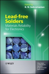
Lead-free Solders (eBook)
John Wiley & Sons (Verlag)
978-1-119-96680-7 (ISBN)
- Phase diagrams and alloy development
- Effect of minor alloying additions
- Composite approaches including nanoscale reinforcements
- Mechanical issues affecting reliability
- Reliability under impact loading
- Thermomechanical fatigue
- Chemical issues affecting reliability
- Whisker growth
- Electromigration
- Thermomigration
Presenting a comprehensive understanding of the current state of lead-free electronic interconnects research, this book approaches the ongoing research from fundamental, applied and manufacturing perspectives to provide a balanced view of the progress made and the requirements which still have to be met.
K. N. Subramanian is Professor of Materials Science and Engineering at Michigan State University. He has been a full-time faculty member at MSU for over 45 years. For the last 15 years he has devoted all his research efforts to lead-free electronic solders.
Providing a viable alternative to lead-based solders is a major research thrust for the electrical and electronics industries - whilst mechanically compliant lead-based solders have been widely used in the electronic interconnects, the risks to human health and to the environment are too great to allow continued widescale usage. Lead-free Solders: Materials Reliability for Electronics chronicles the search for reliable drop-in lead-free alternatives and covers: Phase diagrams and alloy development Effect of minor alloying additions Composite approaches including nanoscale reinforcements Mechanical issues affecting reliability Reliability under impact loading Thermomechanical fatigue Chemical issues affecting reliability Whisker growth Electromigration Thermomigration Presenting a comprehensive understanding of the current state of lead-free electronic interconnects research, this book approaches the ongoing research from fundamental, applied and manufacturing perspectives to provide a balanced view of the progress made and the requirements which still have to be met.
K. N. Subramanian is Professor of Materials Science and Engineering at Michigan State University. He has been a full-time faculty member at MSU for over 45 years. For the last 15 years he has devoted all his research efforts to lead-free electronic solders.
Chapter 1
Reliability of Lead-Free Electronic Solder Interconnects: Roles of Material and Service Parameters
K. N. Subramanian
Department of Chemical Engineering and Materials Science, Michigan State University, East Lansing, MI, 48824-1226, USA
Abstract
This chapter is meant to provide a general overview of the issues affecting the reliability of lead-free electronic solder joints subjected to service environments. It is meant to be an introduction to the various thematic areas that are covered in this book. Hence no attempt to provide references to any of the topics mentioned in this chapter is given at the end of this chapter. Extensive references for each of these topics are cited by the authorities contributing various chapters to this book.
1.1 Material Design for Reliable Lead-Free Electronic Solders Joints
It is important to point out that solder joint is a multicomponent system. Solders used in electronic interconnects are in the joint geometry and its overall response to environmental and in-service parameters are influenced by the constraints present in that configuration. Such a joint has substrates, interface intermetallic compound layers that are necessary to form the necessary bonding, solder matrix with its own individual phases and intermetallic compounds (IMCs). In addition to geometrical issues, processing method used for fabrication of joints and the resultant microstructural features, service parameters encountered, and the response of the solder material to external influences, play significant roles in determining the reliability of the electronic solder joints. The service environments encountered are becoming more severe and the continuous rapid advances in microminiaturization of the electronic packages impose ever-increasing demands on such solder joints. Since solder joints present in modern microelectronics operate at very high homologous temperatures significant microstructural changes such as coarsening of the features present in the joint occur affecting their reliability. Because of the changes in the joint geometry to accomplish the microminiaturization such joints are expected to provide structural integrity in addition to providing electrical pathways. They are also expected to be mechanically compliant to dissipate the stresses that develop during service but be dimensionally stable.
Most of the lead-free solder alloys that are in current use contain significant amounts of tin. Such alloys have the suitable melting temperatures and wetting characteristics for utilization in consumer electronics. Among these, Sn-Ag-Cu alloys have been widely adopted. In order to minimize the deleterious effects of thermally induced coarsening of the phases present within the solder matrix and at the solder/substrate interfaces, and to improve the mechanical properties, several detailed studies on phase stability along with resultant developments have taken place. They have provided strategies involving minor amounts of additional alloying additions, as well as reinforcements to produce composite solders. Some of these approaches also help to improve the reliability of the lead-free solder joints. Since solders have to bond with substrates, the substrate materials and its finish will interact with the solder during the reflow process and during service. Several studies aim at combating reliability issues arising from the coarsening of these reaction products, which are quite often brittle.
The improvements to address problems listed in the last few paragraphs are the main contributions from those studying phase diagrams to develop suitable lead-free solder alloys, alloy additions to improve their service reliability, and composite solders. Such judicial material design to improve the service reliability invariably can take place only with the clear understanding of the service environments in which the electronic packages will be placed and the material response and resultant behaviors that affect their reliability. Joint geometry is an added contributing factor that can aggravate the influence of the service environment. However, such joint design is outside the realm of the material development to meet the challenges. If material design can either alleviate the material processes that affect the joint reliability either completely (or most of it), joint geometry hopefully will have minimal influence on the joint reliability.
The following sections address the material processes that influence the service reliability of lead-free solder joints. Detailed discussions on the developments in these avenues are brought out by world-renowned researchers in these fields in the chapters presented in various thematic areas.
1.2 Imposed Fields and the Solder Joint Responses that Affect Their Reliability
This schematic illustrates damage resulting from multiple fields and their complex interactions. Processes identified in this schematic are EM – electromigration, TM – thermal migration, PF – plastic flow and fracture, JH – Joule heating, CS – current stressing, TMF – thermomechanical fatigue. The scenario presented in this schematic illustrates the complex state of damage accumulation resulting from various fields encountered during service (direct effects: EM, TM, PF), and their mutual interactions (coupled effects: TMF, JH, CS), that affect the reliability of lead-free electronic solder joints.
Even during service these fields are time and position dependent. For example, temperature depends on the environment and Joule heating from the current density that can vary with hills and valleys that form due to electromigration. Similarly, the mechanical stress state will depend on the stresses that develop due to coefficient of thermal expansion (CTE) mismatches between the entities present in the joint, stresses that develop due to atom/ion migration caused by electron wind forces, and externally imposed loads. Among those listed the major damage contributors that affect the reliability of the lead-free electronic solders are (i) mechanical integrity, (ii) thermomechanical fatigue, (iii) whisker growth, (iv) electromigration, and (v) thermomigration. It should be pointed out that this is not an ordered list, and that there are significant mutual interactions between them. Such mutual interactions will become progressively more important with the continued efforts towards microminiaturization of electronic packages. Among the five processes listed above, whisker growth, electromigration, and thermomigration have become reliability concerns mainly due to such miniaturization.
1.3 Mechanical Integrity
An electronic package contains several solder joints and their reliability is what needs to be understood. However, reliability studies carried directly with such complex packages quite often cannot provide the means to evaluate the actual material-related issues that cause the failure, a critical piece of information warranted for material developments. On the other hand, if model system studies are carried out, the model geometries used should be representative of those actually encountered in the electronic packaging. Carrying out studies on bulk solder specimens, without any of the constraints encountered in the joint configuration, will not be of any relevance to what happens in the joints.
Depending on the application the solder joints present in electronic packages may be experiencing different ranges of temperatures. In addition to the heating that results from passage of electric current, ambient conditions encountered during service can play significant roles. The deformation mode of Sn-based solders is highly sensitive to temperature and strain rate. Any reliability modeling should take this issue into account, along with issues of constraints and joint geometry.
Reliability under impact loading is a very important consideration not only for shipping considerations, but also for accidental dropping of a device. Industrial drop tests are carried out to check for the impact reliability during shipping. Charpy-type impact tests where the impact load is delivered to the individual solder ball attached to the substrate are also employed. In a realistic electronic package the impact delivered to some other location is realized by the solder. Hence, such tests cannot provide the necessary information about the detailed stress states, modes of fracture, and so on, that are critical for material design. In addition, there are several scenarios, like in automotive and aerospace applications, where random bumping can cause repeated impact loading.
1.4 Thermomechanical Fatigue (TMF)
Thermal excursions encountered in service cause significant damage to solder joints affecting their service reliability. Several material-related processes occur during heating, cooling, and dwell at temperature extremes. For example, the heating and cooling rates, temperature regime (high/low), temperature difference, dwell times at high- and low-temperature extremes, do significantly affect the integrity of the solder joints. These studies have shown that heating rate is an important contributor affecting the joint reliability. Damage accumulation in solder joints subjected to TMF results from a highly inhomogeneous stress distribution. Such stresses arise from CTE mismatches between various entities present in the joint. Anisotropy of tin could be a major contributing factor for such damage accumulation since the CTE difference between a- and c-directions of body-centered tetragonal β-Sn is almost twice that of the CTE difference between polycrystalline copper and polycrystalline Sn. Manifestation of the damage from TMF occurs only after several hundred TMF cycles,...
| Erscheint lt. Verlag | 6.3.2012 |
|---|---|
| Reihe/Serie | Wiley Series in Materials for Electronic & Optoelectronic Applications |
| Wiley Series in Materials for Electronic & Optoelectronic Applications | Wiley Series in Materials for Electronic & Optoelectronic Applications |
| Sprache | englisch |
| Themenwelt | Naturwissenschaften ► Chemie |
| Technik ► Elektrotechnik / Energietechnik | |
| Technik ► Maschinenbau | |
| Schlagworte | Alternatives • Diagrams • Electrical • Electrical & Electronics Engineering • Electronic materials • Electronics • Elektronische Materialien • Elektrotechnik u. Elektronik • Environment • Great • Halbleiterphysik • Health • Industries • leadfree • Major • Materials • Materials Science • Materialwissenschaften • Mechanically • Physics • Physik • Reliability • reliable dropin • Research • Search • Semiconductor physics • Solders • thrust • Usage • viable alternative • widescale |
| ISBN-10 | 1-119-96680-9 / 1119966809 |
| ISBN-13 | 978-1-119-96680-7 / 9781119966807 |
| Informationen gemäß Produktsicherheitsverordnung (GPSR) | |
| Haben Sie eine Frage zum Produkt? |
Kopierschutz: Adobe-DRM
Adobe-DRM ist ein Kopierschutz, der das eBook vor Mißbrauch schützen soll. Dabei wird das eBook bereits beim Download auf Ihre persönliche Adobe-ID autorisiert. Lesen können Sie das eBook dann nur auf den Geräten, welche ebenfalls auf Ihre Adobe-ID registriert sind.
Details zum Adobe-DRM
Dateiformat: EPUB (Electronic Publication)
EPUB ist ein offener Standard für eBooks und eignet sich besonders zur Darstellung von Belletristik und Sachbüchern. Der Fließtext wird dynamisch an die Display- und Schriftgröße angepasst. Auch für mobile Lesegeräte ist EPUB daher gut geeignet.
Systemvoraussetzungen:
PC/Mac: Mit einem PC oder Mac können Sie dieses eBook lesen. Sie benötigen eine
eReader: Dieses eBook kann mit (fast) allen eBook-Readern gelesen werden. Mit dem amazon-Kindle ist es aber nicht kompatibel.
Smartphone/Tablet: Egal ob Apple oder Android, dieses eBook können Sie lesen. Sie benötigen eine
Geräteliste und zusätzliche Hinweise
Buying eBooks from abroad
For tax law reasons we can sell eBooks just within Germany and Switzerland. Regrettably we cannot fulfill eBook-orders from other countries.
aus dem Bereich


