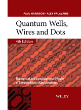
Quantum Wells, Wires and Dots (eBook)
John Wiley & Sons (Verlag)
978-1-118-92334-4 (ISBN)
Quantum Wells, Wires and Dots provides all the essential information, both theoretical and computational, to develop an understanding of the electronic, optical and transport properties of these semiconductor nanostructures. The book will lead the reader through comprehensive explanations and mathematical derivations to the point where they can design semiconductor nanostructures with the required electronic and optical properties for exploitation in these technologies.
This fully revised and updated 4th edition features new sections that incorporate modern techniques and extensive new material including:
- Properties of non-parabolic energy bands
- Matrix solutions of the Poisson and Schrödinger equations
- Critical thickness of strained materials
- Carrier scattering by interface roughness, alloy disorder and impurities
- Density matrix transport modelling
- Thermal modelling
Written by well-known authors in the field of semiconductor nanostructures and quantum optoelectronics, this user-friendly guide is presented in a lucid style with easy to follow steps, illustrative examples and questions and computational problems in each chapter to help the reader build solid foundations of understanding to a level where they can initiate their own theoretical investigations. Suitable for postgraduate students of semiconductor and condensed matter physics, the book is essential to all those researching in academic and industrial laboratories worldwide.
Instructors can contact the authors directly (p.harrison@shu.ac.uk / a.valavanis@leeds.ac.uk) for Solutions to the problems.
Professor Paul Harrison
After his first degree in physics at the University of Hull, Paul decided to pursue an academic career because of his wish to share the love of his subject with students. With that in mind Paul did a a PhD in computational physics at the University of Newcastle-upon-Tyne and then returned to Hull in 1991 to work as a postdoctoral researcher assistant in the Applied Physics department. After four successful years Paul had built his CV up to the level to obtain a five-year research fellowship in 1995 in the School of Electronic & Electrical Engineering at the University of Leeds. This was a strategic move by the University of Leeds to hire early-career researchers and develop them into independent research leaders. The fellowship gave Paul the time to invest heavily in his own research portfolio and Paul built up a group of research students and postdocs, a strong publications track record and an international reputation in theory and design of semiconductor optoelectronic devices.
At the end of his fellowship Paul was promoted to Reader in 2000 and subsequently Professor of Quantum Electronics in 2002. The following year Paul was nominated by the staff to be Head of the School of Electronic and Electrical Engineering, rated 5* in the 2001 Research Assessment Exercise. Under his leadership the school continued to develop its research portfolio and worked as a team to push on with its research strategy: subsequently rewarded by being ranked top of its unit of assessment in the 2008 RAE.
Paul was promoted to Dean of Postgraduate Research Studies in 2011, a university-wide portfolio to develop postgraduate research as part of the overall university strategy. This included responsibility for developing research funding for postgraduate students, marketing, recruitment, admissions and progression, improving submission and completion rates, harmonising processes and improving the student experience across campus. Paul joined Sheffield Hallam University as Pro Vice-Chancellor for Research and Innovation at the start of 2014.
Over his career, Paul has co-authored nearly 300 journal articles, written two books, successfully supervised 16 students to PhD, raised £3m of research funding and Google Scholar gives him a h-index of 33.
Dr Alex Valavanis (MIET) received his MEng (Hons) degree in Electronic Engineering from the University of York and his PhD degree in Electronic and Electrical Engineering from the University of Leeds in 2004 and 2009 respectively.
From 2004-2005 he worked with STFC Daresbury Laboratories, Cheshire, developing X-ray detector systems. From 2005-2009, his PhD with the Quantum Electronics Group in the School of Electronic and Electrical Engineering, University of Leeds, focused on the development of numerical simulations, in C/C++, of quantum-cascade lasers (QCLs) in the silicon-germanium material system. Since 2009, he has worked in the Terahertz (THz) Photonics Laboratory within the same institute, developing new THz imaging and sensing techniques.
Dr Valavanis holds full membership of the IET, and has received awards including the BNFL Peter Wilson Award (2009) for Materials Engineering, the GW Carter prize (2008) for best publication by a PhD student and the FW Carter prize (2009) for best PhD thesis within the School of Electronic and Electrical Engineering.
Professor Paul Harrison After his first degree in physics at the University of Hull, Paul decided to pursue an academic career because of his wish to share the love of his subject with students. With that in mind Paul did a a PhD in computational physics at the University of Newcastle-upon-Tyne and then returned to Hull in 1991 to work as a postdoctoral researcher assistant in the Applied Physics department. After four successful years Paul had built his CV up to the level to obtain a five-year research fellowship in 1995 in the School of Electronic & Electrical Engineering at the University of Leeds. This was a strategic move by the University of Leeds to hire early-career researchers and develop them into independent research leaders. The fellowship gave Paul the time to invest heavily in his own research portfolio and Paul built up a group of research students and postdocs, a strong publications track record and an international reputation in theory and design of semiconductor optoelectronic devices. At the end of his fellowship Paul was promoted to Reader in 2000 and subsequently Professor of Quantum Electronics in 2002. The following year Paul was nominated by the staff to be Head of the School of Electronic and Electrical Engineering, rated 5* in the 2001 Research Assessment Exercise. Under his leadership the school continued to develop its research portfolio and worked as a team to push on with its research strategy: subsequently rewarded by being ranked top of its unit of assessment in the 2008 RAE. Paul was promoted to Dean of Postgraduate Research Studies in 2011, a university-wide portfolio to develop postgraduate research as part of the overall university strategy. This included responsibility for developing research funding for postgraduate students, marketing, recruitment, admissions and progression, improving submission and completion rates, harmonising processes and improving the student experience across campus. Paul joined Sheffield Hallam University as Pro Vice-Chancellor for Research and Innovation at the start of 2014. Over his career, Paul has co-authored nearly 300 journal articles, written two books, successfully supervised 16 students to PhD, raised £3m of research funding and Google Scholar gives him a h-index of 33. Dr Alex Valavanis (MIET) received his MEng (Hons) degree in Electronic Engineering from the University of York and his PhD degree in Electronic and Electrical Engineering from the University of Leeds in 2004 and 2009 respectively. From 2004-2005 he worked with STFC Daresbury Laboratories, Cheshire, developing X-ray detector systems. From 2005-2009, his PhD with the Quantum Electronics Group in the School of Electronic and Electrical Engineering, University of Leeds, focused on the development of numerical simulations, in C/C++, of quantum-cascade lasers (QCLs) in the silicon-germanium material system. Since 2009, he has worked in the Terahertz (THz) Photonics Laboratory within the same institute, developing new THz imaging and sensing techniques. Dr Valavanis holds full membership of the IET, and has received awards including the BNFL Peter Wilson Award (2009) for Materials Engineering, the GW Carter prize (2008) for best publication by a PhD student and the FW Carter prize (2009) for best PhD thesis within the School of Electronic and Electrical Engineering.
Chapter 1
Semiconductors and heterostructures
1.1 The mechanics of waves
De Broglie (see reference [1]) stated that a particle of momentum p has an associated wave of wavelength λ given by:
Thus, an electron in a vacuum at a position r and away from the influence of any electromagnetic potentials could be described by a state function, which is of the form of a wave, i.e.
where t is the time, ω the angular frequency and the modulus of the wave vector is given by:
The quantum mechanical momentum has been deduced to be a linear operator [2] acting upon the wave function ψ, with the momentum p arising as an eigenvalue, i.e.
where
which, when operating on the electron vacuum wave function in equation (1.2), would give the following:
and therefore
Thus the eigenvalue
which, not surprisingly, can be simply manipulated (p = ħk = (h/2π)(2π/λ)) to reproduce de Broglie's relationship in equation (1.1).
Following on from this, classical mechanics gives the kinetic energy of a particle of mass m as:
Therefore it may be expected that the quantum mechanical analogy can also be represented by an eigenvalue equation with an operator:
i.e.
where T is the kinetic energy eigenvalue, and, given the form of ∇ in equation (1.5), then:
When acting upon the electron vacuum wave function, i.e.
then
Thus the kinetic energy eigenvalue is given by:
For an electron in a vacuum away from the influence of electromagnetic fields, the total energy E is just the kinetic energy T. Thus the dispersion or energy versus momentum (which is proportional to the wave vector k) curves are parabolic, just as for classical free particles, as illustrated in Fig. 1.1.
Figure 1.1 The energy versus wave vector (proportional to momentum) curve for an electron in a vacuum
The equation describing the total energy of a particle in this wave description is called the time-independent Schrödinger equation and, for this case with only a kinetic energy contribution, can be summarised as follows:
A corresponding equation also exists that includes the time dependency explicitly; this is obtained by operating on the wave function by the linear operator iħ∂/∂t, i.e.
or
Clearly, this eigenvalue ħω is also the total energy but in a form usually associated with waves, e.g. a photon. These two operations on the wave function represent the two complementary descriptions associated with wave–particle duality. Thus the second, i.e. time-dependent, Schrödinger equation is given by:
1.2 Crystal structure
The vast majority of the mainstream semiconductors have a face-centred cubic Bravais lattice, as illustrated in Fig 1.2. The lattice points are defined in terms of linear combinations of a set of primitive lattice vectors, one choice for which is:
Figure 1.2 The face-centred cubic Bravais lattice
The lattice vectors then follow as the set of vectors:
where α1, α2, and α3 are integers.
The complete crystal structure is obtained by placing the atomic basis at each Bravais lattice point. For materials such as Si, Ge, GaAs, AlAs and InP, this consists of two atoms, one at and the other at , in units of A0.
For the group IV materials, such as Si and Ge, as the atoms within the basis are the same, the crystal structure is equivalent to diamond (see Fig. 1.3 (left)). For III–V and II–VI compound semiconductors such as GaAs, AlAs, InP, HgTe and CdTe, the cation sits on the site and the anion on ; this type of crystal is called the zinc blende structure, after ZnS (see Fig. 1.3 (right)). The only exception to this rule is GaN, and its important InxGa1−xN alloys, which have risen to prominence in recent years due to their use in green and blue light emitting diodes and lasers (see, for example, [3]); these materials have the wurtzite structure (see [4], p. 47).
Figure 1.3 The diamond (left) and zinc blende (right) crystal structures
From an electrostatics viewpoint, the crystal potential consists of a three-dimensional lattice of spherically symmetric ionic core potentials screened by the inner shell electrons (see Fig. 1.4), which are further surrounded by the covalent bond charge distributions that hold everything together.
Figure 1.4 Schematic illustration of the ionic core component of the crystal potential across the {001} planes—a three-dimensional array of spherically symmetric potentials
1.3 The effective mass approximation
Therefore, the crystal potential is complicated; however, using the principle of simplicity,1 imagine that it can be approximated by a constant! Then the Schrödinger equation derived for an electron in a vacuum would be applicable. Clearly, though, a crystal is not a vacuum so allow the introduction of an empirical fitting parameter called the effective mass, m*. Thus the time-independent Schrödinger equation becomes:
and the energy solutions follow as:
This is known as the effective mass approximation and has been found to be very suitable for relatively low electron momenta as occur with low electric fields. Indeed, it is the most widely used parameterisation in semiconductor physics (see any good solid state physics book, e.g. ).[4, 5, 6] Experimental measurements of the effective mass have revealed it to be anisotropic—as might be expected since the crystal potential along, say, the [001] axis is different than along the [111] axis. Adachi [7] collates reported values for GaAs and its alloys; the effective mass in other materials can be found in Landolt and Börnstein [8].
In GaAs, the reported effective mass is around 0.067 m0, where m0 is the rest mass of an electron. Figure 1.5 plots the dispersion curve for this effective mass, in comparison with that of an electron in a vacuum.
Figure 1.5 The energy versus wave vector (proportional to momentum) curves for an electron in GaAs compared to that in a vacuum
1.4 Band theory
It has also been found from experiment that there are two distinct energy bands within semiconductors. The lower band is almost full of electrons and can conduct by the movement of the empty states. This band originates from the valence electron states which constitute the covalent bonds holding the atoms together in the crystal. In many ways, electric charge in a solid resembles a fluid, and the analogy for this band, labelled the valence band, is that the empty states behave like bubbles within the fluid—hence their name, holes.
In particular, the holes rise to the uppermost point of the valence band, and just as it is possible to consider the release of carbon dioxide through the motion of beer in a glass, it is actually easier to study the motion of the bubble (the absence of beer), or in this case the motion of the hole.
In a semiconductor, the upper band is almost devoid of electrons. It represents excited electron states which are occupied by electrons promoted from localised covalent bonds into extended states in the body of the crystal. Such electrons are readily accelerated by an applied electric field and contribute to current flow. This band is therefore known as the conduction band.
Figure 1.6 illustrates these two bands. Notice how the valence band is inverted—this is a reflection of the fact that the ‘bubbles’ rise to the top, i.e. their lowest-energy states are at the top of the band. The energy difference between the two bands is known as the band gap, labelled as Egap on the figure. The particular curvatures used in both bands are indicative of those measured experimentally for GaAs, namely effective masses of around 0.067 m0 for an electron in the conduction band, and 0.6 m0 for a (heavy) hole in the valence band. The convention is to put the zero of the energy at the top of the valence band. Note the extra qualifier ‘heavy’. In fact, there is more than one valence band, and they are distinguished by their different effective masses. Chapter 15 will discuss band structure in more detail; this will be in the context of a microscopic...
| Erscheint lt. Verlag | 29.4.2016 |
|---|---|
| Sprache | englisch |
| Themenwelt | Naturwissenschaften ► Physik / Astronomie ► Atom- / Kern- / Molekularphysik |
| Naturwissenschaften ► Physik / Astronomie ► Elektrodynamik | |
| Naturwissenschaften ► Physik / Astronomie ► Festkörperphysik | |
| Technik ► Elektrotechnik / Energietechnik | |
| Technik ► Maschinenbau | |
| Schlagworte | Electrical & Electronics Engineering • Elektrotechnik u. Elektronik • Excitons • Halbleiter • Halbleiterphysik • Heterostructures • Nanomaterialien • nanomaterials • Nanotechnologie • nanotechnology • Physics • Physik • Pseudopotentials • Quantenpunkt • Quantenwell • Quantum cascade lasers • Quantum dots • quantum wells • Rate Equations • scattering • Semiconductor physics • semiconductors • Thermal Modelling |
| ISBN-10 | 1-118-92334-0 / 1118923340 |
| ISBN-13 | 978-1-118-92334-4 / 9781118923344 |
| Informationen gemäß Produktsicherheitsverordnung (GPSR) | |
| Haben Sie eine Frage zum Produkt? |
Kopierschutz: Adobe-DRM
Adobe-DRM ist ein Kopierschutz, der das eBook vor Mißbrauch schützen soll. Dabei wird das eBook bereits beim Download auf Ihre persönliche Adobe-ID autorisiert. Lesen können Sie das eBook dann nur auf den Geräten, welche ebenfalls auf Ihre Adobe-ID registriert sind.
Details zum Adobe-DRM
Dateiformat: EPUB (Electronic Publication)
EPUB ist ein offener Standard für eBooks und eignet sich besonders zur Darstellung von Belletristik und Sachbüchern. Der Fließtext wird dynamisch an die Display- und Schriftgröße angepasst. Auch für mobile Lesegeräte ist EPUB daher gut geeignet.
Systemvoraussetzungen:
PC/Mac: Mit einem PC oder Mac können Sie dieses eBook lesen. Sie benötigen eine
eReader: Dieses eBook kann mit (fast) allen eBook-Readern gelesen werden. Mit dem amazon-Kindle ist es aber nicht kompatibel.
Smartphone/Tablet: Egal ob Apple oder Android, dieses eBook können Sie lesen. Sie benötigen eine
Geräteliste und zusätzliche Hinweise
Buying eBooks from abroad
For tax law reasons we can sell eBooks just within Germany and Switzerland. Regrettably we cannot fulfill eBook-orders from other countries.
aus dem Bereich


