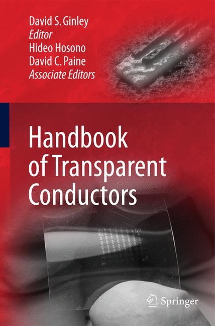
Handbook of Transparent Conductors (eBook)
534 Seiten
Springer US (Verlag)
978-1-4419-1638-9 (ISBN)
Transparent conducting materials are key elements in a wide variety of current technologies including flat panel displays, photovoltaics, organic, low-e windows and electrochromics. The needs for new and improved materials is pressing, because the existing materials do not have the performance levels to meet the ever- increasing demand, and because some of the current materials used may not be viable in the future. In addition, the field of transparent conductors has gone through dramatic changes in the last 5-7 years with new materials being identified, new applications and new people in the field. Handbook of Transparent Conductors presents transparent conductors in a historical perspective, provides current applications as well as insights into the future of the devices. It is a comprehensive reference, and represents the most current resource on the subject.
Handbook of Transparent Conductors 3
Preface 5
Contents 9
Contributors 11
Chapter 1: Transparent Conductors 15
1.1 Basics 15
1.2 History of Transparent Conducting Oxides 22
1.3 Diversity of Transparent Conductors 23
1.4 Emerging Applications 28
1.4.1 Transistors and Flexible Transparent Electronics 28
1.4.2 Electrochromic Windows 30
1.4.3 Optical Arrays 30
1.5 Chapter Topics 31
References 35
Chapter 2: Electronic Structure of Transparent Conducting Oxides 40
2.1 Introduction 40
2.2 Band Structures of n-Type Oxides 40
2.3 Band Structures of p-Type Oxides and Other Cu Oxides 47
2.4 Band Line-ups and Work Functions 51
2.5 Ability to Dope 53
2.6 Effect of Disorder-Disorder in Amorphous Semiconductors 56
2.7 Disorder in Oxide Semiconductors 58
2.8 Summary 60
References 61
Chapter 3: Modeling, Characterization, and Properties of Transparent Conducting Oxides 64
3.1 Introduction 64
3.1.1 A Semi-quantitative Assessment of Grain-Boundary Scattering in TCOs 65
3.1.2 The Free-Electron Theory 68
3.1.3 Application of the Drude Theory 78
3.1.3.1 Determination of the Carrier Concentration 78
3.1.3.2 Estimation of the Relaxation Time 79
Fitting of Spectrophotometer Data 79
Correlation Between Real and Imaginary Parts of Permittivity 81
3.1.3.3 Estimation of the Effective Mass 82
3.2 Measuring Transport Properties in TCOs 84
3.2.1 History of Transport Phenomena 85
3.2.2 Qualitative Review of Transport Phenomena 85
3.2.3 Transport Theory 87
3.2.4 First-Order Non-parabolicity 96
3.2.5 Density-of-States Effective Mass 97
3.2.6 Sample Configuration 101
3.2.7 MFC Results on TCOs 106
3.2.7.1 ZnO (Ionized and Neutral Impurity Scattering) 106
3.2.7.2 Epitaxial ITO and CTO Polycrystalline Films 110
Epitaxial ITO 110
Cadmium Stannate 110
3.3 Improving TCO Figure of Merit Through Improved Optical Performance 113
3.4 Summary 119
References 121
Chapter 4: Characterization of TCO Materials 124
4.1 Introduction 124
4.2 Electrical/Optical Characterization 126
4.2.1 Resistivity Measurements 126
4.2.2 Thickness Determination: X-Ray Reflectivity 127
4.2.3 Hall Measurement of Transport Properties: Hall Mobility and Carrier Density 129
4.2.4 Transistor-Based Transport Measurements 132
4.2.5 Surface Characterization Via Scanning Probe Microscopy 136
4.2.6 Optical Characterization 138
4.2.7 Work Function Measurement 139
4.3 Microstructural/Crystallographic Characterization 141
4.3.1 Crystal Structure and Microstructure: Crystalline Indium Oxide 143
4.3.2 Electron Diffraction Studies of Amorphous In2O3-Based Thin Films 148
4.3.3 Structural Analysis of Amorphous IZO Films 151
4.4 Measurement of Biaxial Stress in TCO Thin Films 155
4.5 Summary 160
References 160
Chapter 5: In Based TCOs 162
5.1 Introduction for In Based TCOs 162
5.2 Crystal Structure and Electronic Structure of In2O3 and Sn Doped In2O3 (ITO) 163
5.3 Electrical and Optical Properties of In2O3-SnO2 Films 166
5.4 Electrical, Optical and Thermal Properties of Amorphous In2O3-ZnO Films 174
References 180
Chapter 6: Transparent Conducting Oxides Based on Tin Oxide 183
6.1 Introduction 183
6.2 Crystal Structure 183
6.3 Chemistry 185
6.4 Physical Properties 187
6.4.1 Band Structure 187
6.4.2 Transport Properties 189
6.4.3 Optical Properties 191
6.4.4 Amorphous SnO2 193
6.4.5 Mechanical Properties and Corrosion Behavior 194
6.5 Thin Film Disposition 194
6.5.1 Substrates 194
6.5.2 Spray Pyrolysis 195
6.5.3 Chemical Vapor Deposition 196
6.5.4 Sputtering 197
6.5.5 Other Deposition Methods 197
6.6 Applications 198
6.6.1 Transparent Thin Film Transistors 198
6.6.2 Gas Sensors 199
6.6.3 Transparent Conductive Oxides 199
6.6.4 Magnetic Properties of SnO2 Semiconductors 200
References 200
Chapter 7: Transparent Conductive Zinc Oxide and Its Derivatives 204
7.1 Introduction 204
7.2 Basic Properties of ZnO 206
7.2.1 Crystallographic Structure 206
7.2.2 Band Structure 207
7.2.3 Thermodynamic Properties 209
7.2.4 Applications of Zinc Oxide 210
7.3 Preparation of Zinc Oxide 211
7.3.1 Single Crystal Growth 211
7.3.2 Thin Film Growth 212
7.3.2.1 Nonreactive Magnetron Sputtering 213
7.3.2.2 Reactive Magnetron Sputtering 215
7.4 Doping and Electrical Transport in ZnO Single Crystals 219
7.4.1 Intrinsic Doping of ZnO 219
7.4.2 Extrinsic n-Type Doping of ZnO 220
7.4.3 Hydrogen in Zinc Oxide 221
7.4.4 Extrinsic p-Type Doping of ZnO 222
7.4.5 Carrier Transport in Single Crystalline ZnO 225
7.4.5.1 Lattice Scattering 225
7.4.5.2 Ionized Impurity Scattering 229
7.4.5.3 Neutral Impurity Scattering 231
7.5 Electrical Transport in Thin Films 232
7.5.1 Transport Models for Polycrystalline Films 232
7.5.1.1 Grain Barrier Limited Transport 232
7.5.1.2 Defect-Limited Transport (Dislocation Scattering) 236
7.5.2 Transport Data for Polycrystalline ZnO Films 237
7.5.2.1 Role of Defects on Transport in ZnO 240
7.5.2.2 Carrier Concentration and Mobility Limits of Degenerately Doped Zinc Oxide 241
7.5.2.3 Transport Data of Epitaxial Films on Different Substrates 242
7.6 Optical Properties of ZnO 247
7.7 Structural and Morphological Properties of Zinc Oxide Films 252
7.8 Zn1-xMexO Alloys 256
7.9 Comparison with Other TCO Materials 262
7.10 Research Opportunities 263
References 265
Chapter 8: Ternary and Multinary Materials: Crystal/Defect Structure-Property Relationships 275
8.1 Introduction 275
8.2 The Role of Cation Coordination 278
8.2.1 Octahedral Cation Coordination (n-Type TCOs) 278
8.2.2 Linear Cation Coordination (p-Type TCOs) 280
8.3 The Role of Defect Complexation 283
8.3.1 Point Defect Complexes in Indium-Tin Oxide 283
8.3.2 Point Defect Complexes in CuAlO2 285
8.3.3 Defect Complexation Summary 289
8.4 Extended Solid Solubility 289
8.5 Limiting Factors for TCOs 293
8.6 Conclusions 299
References 300
Chapter 9: Chemistry of Band Structure Engineering 304
9.1 Introduction 304
9.2 n-Type TCOs 305
9.3 p-Type TCOs 307
9.3.1 ZnO 311
9.3.2 NiO 313
9.3.3 Delafossites 313
9.3.4 Rhodates 315
9.3.5 s Bands for p-Type TCOs 316
9.4 Nonoxides 318
References 318
Chapter 10: Non-conventional Materials 321
10.1 Ultraviolet Transparent TCO: beta-Ga2O3 321
10.1.1 Crystal Structure and Optical Properties 321
10.1.2 Electron Transport and Optical Properties 322
10.1.3 Device Application 324
10.2 Light Metal TCO: 12CaOc7Al2O3 with Built-in Nano-porous Structure 325
10.2.1 Crystal Structure of 12CaO7Al2O3 326
10.2.2 Electronic Structure and Our Approach 327
10.2.3 Electron Doping 328
10.2.3.1 Light-Induced Doping for C12A7:H- 328
10.2.3.2 Doping by Chemical Reduction 330
10.2.3.3 Doping Via Melt Processes 335
10.2.4 Thin Film Fabrication of Electron-Doped C12A7 337
10.2.4.1 Ion Implantation 337
10.2.4.2 Chemical Reduction 340
10.2.5 Unique Properties of Electron-Doped C12A7 and Applications 341
10.2.5.1 Low Work Function 342
10.3 Superconducting Transition [46] 344
10.4 p-Type TCOs 346
10.4.1 Materials Design of p-Type TCOs [52-54] 346
10.4.2 Bipolar Transparent TCOs 348
10.4.3 Layered Oxychalcogenides: Improved p-Type Performance 349
10.4.3.1 Crystal Structure and Epitaxial Film Fabrication: Reactive Solid-Phase Epitaxy 350
10.4.3.2 Carrier Transport, Light Emission and Excitonic Properties 351
10.4.3.3 Two-Dimensional Electronic Structure in LnCuOCh 353
10.5 Summary 355
References 356
Chapter 11: Applications of Transparent Conductors to Solar Energy and Energy Efficiency 360
11.1 Introduction 360
11.2 Foundations for Solar Energy Materials 362
11.2.1 Spectral and Angular Selectivity of Ambient Radiation 362
11.2.2 The Potential of Chromogenic Technologies 364
11.2.3 Substrates for Transparent Conductors, and Their Antireflection Treatment 365
11.3 Applications Based on Spectral Selectivity 367
11.3.1 Metal Based Thin Films for Energy Efficient Windows 369
11.3.1.1 Single-Layer Films 369
11.3.1.2 Multi-layer Films 373
11.3.2 Doped Oxide Based Thin Films for Energy Efficient Windows 375
11.3.2.1 Introduction 375
11.3.2.2 Theoretical Considerations 378
11.3.2.3 Some Empirical Results 383
11.3.3 Diverse Applications of Spectrally Selective Coatings 385
11.3.3.1 Low-Emittance Coatings for Vacuum Glazings 385
11.3.3.2 Doped Tin Oxide Based Thin Films for Avoiding Radiative Cooling 386
11.3.3.3 Comments on Photocatalytic Properties, Self-Cleaning, and Super-hydrophilicity of Transparent Conductors 387
11.3.3.4 Transparent Conductors for Solar Cells 388
11.3.3.5 Doped Oxide Based Thin Films for Solar Collectors 390
11.4 Applications Based on Angular Selectivity 391
11.4.1 General Considerations 391
11.4.2 Data on Obliquely Deposited Cr Based Films 394
11.5 Applications Based on Temporal Variability (Chromogenics) 397
11.5.1 Brief Survey of Chromogenic Materials and Devices 397
11.5.2 Thermochromic Vanadium Dioxide Films 398
11.5.2.1 Basics 398
11.5.2.2 Towards Practical Applications in Energy Efficient Fenestration 400
11.5.3 Electrochromic Oxide Based Films and Devices 402
11.5.3.1 Introduction 402
11.5.3.2 Films of Tungsten Oxide and Nickel Oxide 404
11.5.3.3 Flexible Electrochromic Foils 406
11.6 Concluding Remarks and Futures Issues 409
11.6.1 Materials 409
11.6.2 Applications 411
References 413
Chapter 12: Nanostructured TCOs (ZnO, TiO2, and Beyond) 431
12.1 Other Applications of TCOs 431
12.1.1 Building Applications 432
12.1.2 Organic Photovoltaics 432
12.1.3 Dye Sensitized Solar Cell 434
12.2 TCO Requirements 435
12.2.1 Work Function 435
12.2.2 Surface Chemistry 435
12.2.3 Surface States 435
12.2.4 Organic Interface 436
12.2.5 Etchability 436
12.2.6 Stability 436
12.2.7 Photochemistry 437
12.2.8 Transport 437
12.3 The Hybrid OPV Example 437
12.3.1 Bulk Heterojunction Polymer/ZnO Nanoparticle Solar Cells 437
12.3.2 Ordered Polymer/ZnO Nanorod Array Solar Cells 438
12.3.3 Inverted P3HT:PCBM Bulk Heterojunction Devices Based on ZnO 445
12.3.4 Increasing Charge Collection: P3HT:PCBM/ZnO Nanorod Devices 445
12.3.5 ZnMgO Alloys in Hybrid PV Cells 446
12.4 Dye-Sensitized Solar Cells Using Nanoparticle TiO2 451
12.4.1 3D Structure 451
12.4.2 Conductivity 452
12.4.3 Transport 453
12.5 Next Generation Coatings 453
12.5.1 Superhydrophylic TiO2 454
12.6 Novel Heterostructures 454
12.6.1 From OLEDs to Fuel Cells and Displays 454
12.6.2 New Electro-Optical Devices 455
12.7 New Nanostructured TCO Materials 455
12.7.1 Carbon Nanotube Composites 455
References 456
Chapter 13: Transparent Amorphous Oxide Semiconductors for Flexible Electronics 464
13.1 History of Amorphous Semiconductor 464
13.2 Material Design for Ionic Amorphous Oxide Semiconductors with Large Electron Mobility [11-13] 466
13.3 Example of Transparent TAOS 469
13.4 Unique Electron Transport Properties of TAOS 470
13.5 TAOS in the System In2O3-Ga2O3-ZnO and Their Application to Flexible Transistor 473
13.5.1 Transport Properties 473
13.5.2 Electronic Structure [44] 475
13.5.3 TFT Application 476
13.6 Amorphous TCOs 479
13.6.1 Why Amorphous TCOs 479
13.6.2 Advantage of Binary Oxides 480
13.6.3 General Electron Transport Properties 481
13.6.4 Nano-fabrication [58, 59] 482
13.7 TFT Device Application 483
13.7.1 Unique Features of TAOS-TFTs 484
13.7.2 Novel Display Structure 485
13.7.3 Driving Backplane of OLED and LCD Panels 486
13.8 Future Challenge and Opportunity 488
References 490
Chapter 14: Junctions 493
14.1 Introduction 493
14.2 p-n Junction Diodes 493
14.3 Transparent Diodes 495
14.4 Transparent Photovoltaic Devices 498
14.5 Light-Emitting Diodes 500
14.6 Summary 507
References 509
Chapter 15: Process Technology and Industrial Processes 510
15.1 Challenges to Lower Resistivities 510
15.2 Comparison of Methods for the Uniform Large Area Deposition 512
15.3 Two-Source Evaporation 513
15.3.1 Spatial Distribution of Evaporated Substance 514
15.3.2 Calculation of the Thickness Distribution 516
15.3.3 Large Area Deposition from Two Point Sources 517
15.4 Sputter Deposition 518
15.5 Transparent Electrode for Large Area Solar Cells 521
15.5.1 Properties Requested to Textured TCOs 522
15.5.2 The Present State of the Art of SnO2:F TCO 524
15.5.3 CVD Deposition of SnO2:F TCOs 526
15.5.4 Present State of the Art of ZnO TCOs 527
References 528
Index 530
| Erscheint lt. Verlag | 11.9.2010 |
|---|---|
| Mitarbeit |
Stellvertretende Herausgeber: Hideo Hosono, David C. Paine |
| Zusatzinfo | XIV, 534 p. 107 illus. in color. |
| Verlagsort | New York |
| Sprache | englisch |
| Themenwelt | Naturwissenschaften ► Chemie ► Analytische Chemie |
| Naturwissenschaften ► Chemie ► Physikalische Chemie | |
| Naturwissenschaften ► Physik / Astronomie ► Elektrodynamik | |
| Technik ► Elektrotechnik / Energietechnik | |
| Technik ► Maschinenbau | |
| ISBN-10 | 1-4419-1638-5 / 1441916385 |
| ISBN-13 | 978-1-4419-1638-9 / 9781441916389 |
| Informationen gemäß Produktsicherheitsverordnung (GPSR) | |
| Haben Sie eine Frage zum Produkt? |
Größe: 17,8 MB
DRM: Digitales Wasserzeichen
Dieses eBook enthält ein digitales Wasserzeichen und ist damit für Sie personalisiert. Bei einer missbräuchlichen Weitergabe des eBooks an Dritte ist eine Rückverfolgung an die Quelle möglich.
Dateiformat: PDF (Portable Document Format)
Mit einem festen Seitenlayout eignet sich die PDF besonders für Fachbücher mit Spalten, Tabellen und Abbildungen. Eine PDF kann auf fast allen Geräten angezeigt werden, ist aber für kleine Displays (Smartphone, eReader) nur eingeschränkt geeignet.
Systemvoraussetzungen:
PC/Mac: Mit einem PC oder Mac können Sie dieses eBook lesen. Sie benötigen dafür einen PDF-Viewer - z.B. den Adobe Reader oder Adobe Digital Editions.
eReader: Dieses eBook kann mit (fast) allen eBook-Readern gelesen werden. Mit dem amazon-Kindle ist es aber nicht kompatibel.
Smartphone/Tablet: Egal ob Apple oder Android, dieses eBook können Sie lesen. Sie benötigen dafür einen PDF-Viewer - z.B. die kostenlose Adobe Digital Editions-App.
Buying eBooks from abroad
For tax law reasons we can sell eBooks just within Germany and Switzerland. Regrettably we cannot fulfill eBook-orders from other countries.
aus dem Bereich


