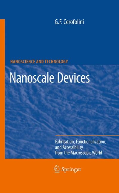
Nanoscale Devices (eBook)
XVI, 205 Seiten
Springer Berlin (Verlag)
978-3-540-92732-7 (ISBN)
Gianfranco ('GF') Cerofolini (degree in Physics from the University of Milan, 1970) is visiting researcher at the University of Milano-Bicocca. His major interests are addressed to the physical limits of miniaturization and to the 'emergence' of higher-level phenomena from the underlying lower-level substrate (measurement in quantum mechanics, life in biological systems, etc.).
Although his research activity has been carried out in the industry (vacuum: SAES Getters; telecommunication: Telettra; chemistry and energetics: ENI; integrated circuits: STMicroelectronics), he has had frequent collaborations with academic centers (University of Lublin, IMEC, Stanford University, City College of New York, several Italian Universities), has been lecturer in a few Universities (Pisa, Modena, and Polytechnic of Milan), and currently is lecturer at the University of Milano-Bicocca.
His research has covered several areas: adsorption, biophysics, CMOS processing (oxidation, diffusion, ion implantation, gettering), electronic and optical materials, theory of acidity, and nanoelectronics.
A gettering technique of widespread use in microelectronics, the complete setting of ST's first silicon-gate CMOS process, the development of a process for low-fluence SOI, and the identification of a strategy for molecular electronics via a conservative extension of the existing microelectronic technology, are among his major industrial achievements. His main scientific results range from the preparation and characterization of ideal silicon p-n junctions and the discovery of a mechanism therein of pure generation without recombination, to the theoretical description of layer-by-layer oxidation at room temperature of silicon, and to the development of original mathematical techniques for the description of adsorption on heterogeneous or soft surfaces.
The results of his activity have been published in approximately 300 articles, chapters to books, and encyclopaedic items, and in a score of patents.
Gianfranco ("GF") Cerofolini (degree in Physics from the University of Milan, 1970) is visiting researcher at the University of Milano-Bicocca. His major interests are addressed to the physical limits of miniaturization and to the 'emergence' of higher-level phenomena from the underlying lower-level substrate (measurement in quantum mechanics, life in biological systems, etc.). Although his research activity has been carried out in the industry (vacuum: SAES Getters; telecommunication: Telettra; chemistry and energetics: ENI; integrated circuits: STMicroelectronics), he has had frequent collaborations with academic centers (University of Lublin, IMEC, Stanford University, City College of New York, several Italian Universities), has been lecturer in a few Universities (Pisa, Modena, and Polytechnic of Milan), and currently is lecturer at the University of Milano-Bicocca. His research has covered several areas: adsorption, biophysics, CMOS processing (oxidation, diffusion, ion implantation, gettering), electronic and optical materials, theory of acidity, and nanoelectronics. A gettering technique of widespread use in microelectronics, the complete setting of ST's first silicon-gate CMOS process, the development of a process for low-fluence SOI, and the identification of a strategy for molecular electronics via a conservative extension of the existing microelectronic technology, are among his major industrial achievements. His main scientific results range from the preparation and characterization of ideal silicon p-n junctions and the discovery of a mechanism therein of pure generation without recombination, to the theoretical description of layer-by-layer oxidation at room temperature of silicon, and to the development of original mathematical techniques for the description of adsorption on heterogeneous or soft surfaces. The results of his activity have been published in approximately 300 articles, chapters to books, and encyclopaedic items, and in a score of patents.
Preface 7
Contents 10
List of Acronyms 14
Part I Basics 16
1 Matter on the Nanoscale 17
1.1 Nanotechnology and the (N+ 1) Problem 18
1.2 Microelectronics is a Nanotechnology 19
1.3 From Microlectronics to Molecular Electronics 20
2 Top-Down Paradigm to Miniaturization 22
2.1 The Path Toward Size Reduction 23
2.2 Going Down with Device Size is a Hard Uphill Path 27
2.2.1 The Physical Limit 27
2.2.2 The Technological Limit 28
2.2.3 The Economic Limit 29
2.3 Going Beneath the Limiting Size 30
3 Physical Limits to Miniaturization 32
3.1 A Case Study: The Limits of Computation 32
3.2 The Basic Computational Unit 33
3.3 Programming 37
3.3.1 Limits Imposed by the Uncertainty Principle 37
3.3.2 Limits Imposed by Ballistic Material Motion 38
3.3.3 Limits Imposed by the Thermal Embedding 39
3.4 Computation and Irreversibility 42
3.4.1 Irreversible Computation 42
3.4.2 Reversible Computation 43
3.4.3 Minimum Dissipation 45
3.4.4 Computation and Measure 49
3.5 Reading 52
3.5.1 Coupling the Carrier with the External World 53
3.5.2 Physical Limits in read Operation 53
3.5.3 A Little Step Toward Practical Implementation 57
4 The Crossbar Structure 58
4.1 The Crossbar Process 59
4.2 Process Integration 63
4.3 Why Molecules? 64
5 Crossbar Production 66
5.1 Imprint Lithography 67
5.2 Spacer Patterning Technology 69
5.3 Multispacer Patterning Technology 69
5.3.1 Multiplicative Route: SnPT 70
5.3.2 Additive Route: SnPT+ 74
5.4 Minimum Exploitable Bar Width 80
6 The Litho-to-Nano link 82
6.1 The Horizontal Beveling Technique 84
6.2 Fusing Adjacent Lines in SnPT+ 85
6.3 Energetic Filtering 88
6.4 Technology and Architecture 90
6.5 Not Only Crossbars 92
6.5.1 Supercapacitors 93
6.5.2 Photoluminescent Nanosheets 93
6.5.3 Nanowire Arrays as Seebeck Generators 94
7 Functional Molecules 96
7.1 The Molecule as a One-Dimensional Wire 96
7.1.1 The Role of Contacts: Landauer Resistance 97
7.1.2 Barrier Transparency 97
7.2 Conduction Along Alkanes 100
7.3 Switchable -Conjugated Molecules 101
7.4 Molecules Exhibiting Superexchange Conduction 103
7.5 A Comparison of the Switching Mechanisms 105
8 Grafting Functional Molecules 107
8.1 Silicon and Its Surfaces 107
8.1.1 Silicon Chemistry 109
8.1.2 The Role of Surfaces 110
8.1.3 The Surface of Single-Crystalline Silicon 111
8.1.4 The Surface of Polycrystalline Silicon 117
8.1.5 The Surface of Porous Silicon 118
8.1.6 Inner Surfaces and the Fantastic Chemistryin Nanocavities 119
8.2 Routes for Silicon Functionalization 123
8.2.1 Hydrosilation 125
8.2.2 Hydrosilation at the Hydrogen-Terminated (1 0 0) Si Surface 126
8.3 Grafting in Restricted Geometries 128
8.4 Three-Terminal Molecules 135
8.5 Nanostructured Oxo-Bonded Silicon 137
8.5.1 Hydrothermal Synthesis: Zeolites 138
8.5.2 Hydrolysis and Polycondensation: Aerogels 139
Concluding Remarks 142
Part II Advanced Topics: Self-Similar Structures, Molecular Motors, and Nanobiosystems 143
9 Examples 144
9.1 Hybrid Molecule–MOS-FET Combination 144
9.2 Crossbar Functionalization 146
10 Self-Similar Nanostructures 150
10.1 Fractals 150
10.1.1 Queer Systems 150
10.1.2 Fractals in Mathematics 151
10.2 Fractals in Nature 152
10.2.1 Fractal Biological Systems 152
10.2.2 Fractal Surfaces 153
10.3 Fractals in Technology 155
11 Molecular Motors 159
11.1 Molecular Building Blocks 161
11.2 Controlling Movement with Electric Field 163
11.3 Combining Ballistic and Brownian Motions 165
11.4 Brownian Motors 168
12 Nanobiosensing 172
12.1 Reducing Cell Biology to Molecular Biology 172
12.2 From Molecular Biology to Systems Biology 175
12.3 Sensing as a Key Tool for Systems Biology 176
12.4 From ICs to Nanobiosensors 177
12.4.1 The Incremental Increase of Complexityof ICs and Sensors 178
12.4.2 The Shift of Paradigm 179
12.5 A Roadmap for Nanobiosensing 181
12.5.1 Nanobiosensing In Vitro 181
12.5.2 Nanobiosensing In Vivo 184
13 Abstract Technology 186
13.1 Material Bodies and Surfaces 187
13.2 Processes Controlled by Geometry 188
13.2.1 Conformal Processes 189
13.2.2 Directional Processes 191
13.3 Processes Controlled by the Material 193
13.4 Abstract Technology in Concrete 195
References 198
Index 208
About the Author 212
| Erscheint lt. Verlag | 26.8.2009 |
|---|---|
| Reihe/Serie | NanoScience and Technology |
| Zusatzinfo | XVI, 205 p. 84 illus., 54 illus. in color. |
| Verlagsort | Berlin |
| Sprache | englisch |
| Themenwelt | Naturwissenschaften ► Physik / Astronomie |
| Technik ► Elektrotechnik / Energietechnik | |
| Technik ► Maschinenbau | |
| Schlagworte | Batch access to the molecular world • biosensing • Electronics • Fabrication • Molecular electronics • Nanobiointerface • Nanoscience • nanostructure • nanotechnology |
| ISBN-10 | 3-540-92732-8 / 3540927328 |
| ISBN-13 | 978-3-540-92732-7 / 9783540927327 |
| Haben Sie eine Frage zum Produkt? |
Größe: 6,2 MB
DRM: Digitales Wasserzeichen
Dieses eBook enthält ein digitales Wasserzeichen und ist damit für Sie personalisiert. Bei einer missbräuchlichen Weitergabe des eBooks an Dritte ist eine Rückverfolgung an die Quelle möglich.
Dateiformat: PDF (Portable Document Format)
Mit einem festen Seitenlayout eignet sich die PDF besonders für Fachbücher mit Spalten, Tabellen und Abbildungen. Eine PDF kann auf fast allen Geräten angezeigt werden, ist aber für kleine Displays (Smartphone, eReader) nur eingeschränkt geeignet.
Systemvoraussetzungen:
PC/Mac: Mit einem PC oder Mac können Sie dieses eBook lesen. Sie benötigen dafür einen PDF-Viewer - z.B. den Adobe Reader oder Adobe Digital Editions.
eReader: Dieses eBook kann mit (fast) allen eBook-Readern gelesen werden. Mit dem amazon-Kindle ist es aber nicht kompatibel.
Smartphone/Tablet: Egal ob Apple oder Android, dieses eBook können Sie lesen. Sie benötigen dafür einen PDF-Viewer - z.B. die kostenlose Adobe Digital Editions-App.
Zusätzliches Feature: Online Lesen
Dieses eBook können Sie zusätzlich zum Download auch online im Webbrowser lesen.
Buying eBooks from abroad
For tax law reasons we can sell eBooks just within Germany and Switzerland. Regrettably we cannot fulfill eBook-orders from other countries.
aus dem Bereich


