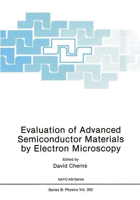
Evaluation of Advanced Semiconductor Materials by Electron Microscopy
Kluwer Academic / Plenum Publishers (Verlag)
978-0-306-43362-7 (ISBN)
- Titel ist leider vergriffen;
keine Neuauflage - Artikel merken
High Resolution Electron Microscopy.- HREM of Edge-on Interfaces and Defects.- Image Processing Applied to HRTEM Images of Interfaces.- II-VI Semiconductor Interfaces.- High Resolution Electron Microscopy Study of Indium Distribution in InAs/GaAs Multilayers.- Convergent Beam Electron Diffraction.- Convergent Beam Electron Diffraction Studies of Defects, Strains and Composition Profiles in Semiconductors.- HOLZ Diffraction from Semiconductor Superlattices.- Determination of Composition and Ionicity by Critical Voltage and Other Electron Diffraction Methods.- Measurement of Structure-Factor Phases by Electron Diffraction for the Study of Bonding in Non-Centrosymmetric Semiconductors.- X-ray and Electron Energy Loss Microanalysis.- EDX and EELS Studies of Segregation in STEM.- Cathodoluminescence and Electron Beam Induced Conductivity.- TEM-Cathodoluminescence Study of Single and Multiple Quantum Wells of MBE Grown GaAs/AlGaAs.- EBIC Studies of Individual Defects in Lightly Doped Semiconductors CdTe as an Example.- Schottky Barriers.- Electronic Structure and Fermi Level Pinning Obtained with Spatially Resolved Electron Energy Loss Scattering.- Epitaxial NiSi2 and CoSi2 Interfaces.- Further Analysis of Interfaces.- The Fresnel Method for the Characterisation of Interfaces.- Strains and Misfit Dislocations at Interfaces.- Ordering/decomposition/analysis of local strains.- TEM and STEM Observations of Composition Variations in III-V Semiconductors.- Transmission Electron Microscopy and Transmission Electron Diffraction Studies of Atomic Ordering in Group III-V Compound Semiconductor Alloys.- Elastic Relaxation and TEM Image Contrasts in Thin Composition-Modulated Semiconductor Crystals.- Surface Microscopy and Diffraction.- Surface and Thin Film Growth Studied by Reflection High Energy Electron Diffraction.- Low Energy Electron Microscopy (LEEM) and Photoemission Microscopy (PEEM) of Semiconductor Surfaces.- Transmission Electron Microscopy of In-Situ Deposited Films on Silicon.- Surface Studies by SEM and STEM.- Transmission and Reflection Electron Microscopy on Cleaved Edges of III-V Multilayered Structures.- Defects in Heteroepitaxy.- Dislocation Generation and Elimination in GaAs on Si.- The Microstructure of GaAs/Si Films Studied as a Function of Heat Treatment.- Electron Microscopy of Gex Sil-x/Si Strained Layer Superlattices.- Defect Structure in Low and High Misfit Systems.- In-Situ Electron Microscope Studies of Misfit Dislocation Introduction into Gex Sil-x/Si Heterostructures.- Misfit Dislocations in Inx Gal-x As/GaAs Heterostructures near the Critical Thickness.- Summary of Discussion on Instrumental Requirements for the Evaluation of Advanced Semiconductors by Electron Microscopy.
| Erscheint lt. Verlag | 1.1.1990 |
|---|---|
| Reihe/Serie | NATO Science Series: B ; 203 |
| Zusatzinfo | 412 p. |
| Verlagsort | Dordrecht |
| Sprache | englisch |
| Gewicht | 920 g |
| Themenwelt | Medizin / Pharmazie ► Studium |
| Naturwissenschaften ► Physik / Astronomie ► Festkörperphysik | |
| ISBN-10 | 0-306-43362-1 / 0306433621 |
| ISBN-13 | 978-0-306-43362-7 / 9780306433627 |
| Zustand | Neuware |
| Informationen gemäß Produktsicherheitsverordnung (GPSR) | |
| Haben Sie eine Frage zum Produkt? |
aus dem Bereich


