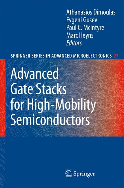
Advanced Gate Stacks for High-Mobility Semiconductors (eBook)
XXII, 384 Seiten
Springer Berlin (Verlag)
978-3-540-71491-0 (ISBN)
This book provides a comprehensive monograph on gate stacks in semiconductor technology. It covers the major latest developments and basics and will be useful as a reference work for researchers, engineers and graduate students alike. The reader will get a clear view of what has been done so far, what is the state-of-the-art and which are the main challenges ahead before we come any closer to a viable Ge and III-V MOS technology.
Dr. Dimoulas obtained his Ph.D in Applied Physics from the University of Crete and the Foundation for Research &Technology-Hellas (FORTH), Greece in 1991 for his research on heteroepitaxial strain of III-V semiconductors grown on Si by MBE. He worked in the Microelectronics Research Group of FORTH until 1992. He was Human Capital & Mobility Fellow of the EU at the University of Groningen, Holland until 1994, a Research Fellow at the California Institute of Technology (CALTECH), Chemical Engineering, Pasadena USA until1996 and member of the Faculty at the University of Maryland at College Park (UMCP) USA, until February 1999. In addition, he has been visiting research scientist at NRL, Washington DC in 1992 and at IBM Zurich Research Laboratory, Switzerland in 2006. Since 1999, he is research director and head of the MBE laboratory at the Institute of Materials Science of the National Center for Scientific Research DEMOKRITOS, Athens, Greece. He is leading several European-funded projects in the areas of advanced microelectronic materials and devices. He has co-author more than 80 publications in international journals, archives and proceedings, and has also written book chapters. He has given 15 invited presentations during the last five years. He has been involved in the organization of several conferences and workshops either as the main organizer or as a member of advisory and program committees. Finally, he is reviewer in recognized International Journals and evaluator of research and development projects. His expertise includes MBE growth of Semiconductor and dielectric materials (high-k oxides), nanodevice processing by e-beam lithography and materials characterization and device electrical testing. His current interests focus on advanced high-k gate stacks for Ge and III-V MOS technology
Dr. Evgeni Gusev received his MS (Applied Physics/Molecular Physics) and PhD (Solid State Physics) from Moscow Engineering Physics Institute - Technical University in 1988 and 1991. In 1993, he joined Laboratory for Surface Modifications at Rutgers University, first as a PostDoctoral Fellow and then as a Research Assistant Professor, where he established a program on fundamental aspects of gate dielectrics. In 1997, following the invitation by Prof. Masataka Hirose, he held an appointment of Visiting Professor in the Center for Nanodevices and Systems in Hiroshima University, Japan. Shortly after that he moved to IBM, where he was responsible for several projects on gate stack processing, characterization, and FEOL device integration (starting from 0.25um CMOS to 32 nm devices more recently) in both IBM Semiconductor Research and Development Center (SRDC) in East Fishkill (NY) and IBM T.J. Watson Research Center in Yorktown Heights (NY). In July 2005, he joined QUALCOMM MEMS Technology Development Center in San Jose as the Director of Research and Development. Since 2004, he is also a Distinguished Visiting Professor at Rutgers University. Dr. Gusev has contributed to the technical R&D community with 10 edited books, more than 150 publications and 20 issued and filed patents on various aspects of semiconductor devices and technology. He is a member of several international professional committees, panels and societies.
Professor Paul McIntyre is Associate Professor of Materials Science and Engineering and Deputy Director of the Geballe Laboratory for Advanced Materials at Stanford University. McIntyre leads a research team of fourteen graduate students, three visiting scientists, and two consulting professors who perform basic research on nanostructured inorganic materials for applications in electronics, energy technologies and sensors. He is best known for his work on metal oxide/semiconductor interfaces, ultrathin high-k dielectrics, defects in complex metal oxide thin films, and nanostructured Si-Ge single crystals. His research team synthesizes materials, characterizes their structures and compositions with a variety of advanced microscopies and spectroscopies, studies the passivation of their interfaces, and measures functional properties of devices. Their research is supported by several U.S. government agencies and major semiconductor manufacturers world-wide. McIntyre is an author of approximately 100 archival journal papers and inventor of 5 US patents, and has given over 60 invited presentations, plenary talks and tutorial lectures. He has received an IBM Faculty Award and Charles Lee Powell Foundation Faculty Scholarship in recognition of his group's research. Prior to joining Stanford, McIntyre was a member of the technical staff in the Central Research Laboratories at Texas Instruments and he also served as Lab Director's Fund Postdoctoral Fellow in the Materials Division at Los Alamos National Laboratory. He earned the Sc.D. from the Materials Science and Engineering department at MIT and the B.A.Sc. from the Materials Engineering department at the University of British Columbia (Canada). McIntyre is a technical advisor to Unity Semiconductor Corporation, and has been an invited member of government and industry panels studying future research needs in ceramic materials, metal oxide/semiconductor structures, nano-scale ferroelectrics and nano-electronics.
Professor Dr. Marc Heyns was born in Turnhout, Belgium, on November 16, 1956. He received the M.S. degree in Applied Sciences (Electronics) in 1979 from the Katholieke Universiteit Leuven, Belgium. In 1986 he received the Ph.D. degree, also from the Katholieke Universiteit Leuven, Belgium, with a thesis entitled: 'Study of the charge trapping and degradation of thermally grown SiO2 layers'. From 1979 to 1985 he held a fellowship from the National Fund for Scientific Research (NFWO) in the Laboratory for Physics and Electronics of Semiconductors of the K.U. Leuven. In January 1986 he joined IMEC where he became Department Director and Program Director responsible for a research group working on ultra-clean processing technology, advanced high-k gate stacks, metal gates, epitaxial deposition of materials, environmentally benign processing and novel high-mobility substrate materials. He became an IMEC-Fellow in 2001 and a Professor at the Katholieke Universiteit Leuven in 2005. He has authored or co-authored more than 150 contributions in scientific journals and more than 500 papers at international conferences. His current research topics include novel high-k dielectric materials, advanced cleaning and surface preparation technology, epitaxy, novel devices made on high-mobility substrates such Ge and III/V compounds, nanowires and carbon nanotubes.
Dr. Dimoulas obtained his Ph.D in Applied Physics from the University of Crete and the Foundation for Research &Technology-Hellas (FORTH), Greece in 1991 for his research on heteroepitaxial strain of III-V semiconductors grown on Si by MBE. He worked in the Microelectronics Research Group of FORTH until 1992. He was Human Capital & Mobility Fellow of the EU at the University of Groningen, Holland until 1994, a Research Fellow at the California Institute of Technology (CALTECH), Chemical Engineering, Pasadena USA until1996 and member of the Faculty at the University of Maryland at College Park (UMCP) USA, until February 1999. In addition, he has been visiting research scientist at NRL, Washington DC in 1992 and at IBM Zurich Research Laboratory, Switzerland in 2006. Since 1999, he is research director and head of the MBE laboratory at the Institute of Materials Science of the National Center for Scientific Research DEMOKRITOS, Athens, Greece. He is leading several European-funded projects in the areas of advanced microelectronic materials and devices. He has co-author more than 80 publications in international journals, archives and proceedings, and has also written book chapters. He has given 15 invited presentations during the last five years. He has been involved in the organization of several conferences and workshops either as the main organizer or as a member of advisory and program committees. Finally, he is reviewer in recognized International Journals and evaluator of research and development projects. His expertise includes MBE growth of Semiconductor and dielectric materials (high-k oxides), nanodevice processing by e-beam lithography and materials characterization and device electrical testing. His current interests focus on advanced high-k gate stacks for Ge and III-V MOS technology Dr. Evgeni Gusev received his MS (Applied Physics/Molecular Physics) and PhD (Solid State Physics) from Moscow Engineering Physics Institute – Technical University in 1988 and 1991. In 1993, he joined Laboratory for Surface Modifications at Rutgers University, first as a PostDoctoral Fellow and then as a Research Assistant Professor, where he established a program on fundamental aspects of gate dielectrics. In 1997, following the invitation by Prof. Masataka Hirose, he held an appointment of Visiting Professor in the Center for Nanodevices and Systems in Hiroshima University, Japan. Shortly after that he moved to IBM, where he was responsible for several projects on gate stack processing, characterization, and FEOL device integration (starting from 0.25um CMOS to 32 nm devices more recently) in both IBM Semiconductor Research and Development Center (SRDC) in East Fishkill (NY) and IBM T.J. Watson Research Center in Yorktown Heights (NY). In July 2005, he joined QUALCOMM MEMS Technology Development Center in San Jose as the Director of Research and Development. Since 2004, he is also a Distinguished Visiting Professor at Rutgers University. Dr. Gusev has contributed to the technical R&D community with 10 edited books, more than 150 publications and 20 issued and filed patents on various aspects of semiconductor devices and technology. He is a member of several international professional committees, panels and societies. Professor Paul McIntyre is Associate Professor of Materials Science and Engineering and Deputy Director of the Geballe Laboratory for Advanced Materials at Stanford University. McIntyre leads a research team of fourteen graduate students, three visiting scientists, and two consulting professors who perform basic research on nanostructured inorganic materials for applications in electronics, energy technologies and sensors. He is best known for his work on metal oxide/semiconductor interfaces, ultrathin high-k dielectrics, defects in complex metal oxide thin films, and nanostructured Si-Ge single crystals. His research team synthesizes materials, characterizes their structures and compositions with a variety of advanced microscopies and spectroscopies, studies the passivation of their interfaces, and measures functional properties of devices. Their research is supported by several U.S. government agencies and major semiconductor manufacturers world-wide. McIntyre is an author of approximately 100 archival journal papers and inventor of 5 US patents, and has given over 60 invited presentations, plenary talks and tutorial lectures. He has received an IBM Faculty Award and Charles Lee Powell Foundation Faculty Scholarship in recognition of his group’s research. Prior to joining Stanford, McIntyre was a member of the technical staff in the Central Research Laboratories at Texas Instruments and he also served as Lab Director’s Fund Postdoctoral Fellow in the Materials Division at Los Alamos National Laboratory. He earned the Sc.D. from the Materials Science and Engineering department at MIT and the B.A.Sc. from the Materials Engineering department at the University of British Columbia (Canada). McIntyre is a technical advisor to Unity Semiconductor Corporation, and has been an invited member of government and industry panels studying future research needs in ceramic materials, metal oxide/semiconductor structures, nano-scale ferroelectrics and nano-electronics. Professor Dr. Marc Heyns was born in Turnhout, Belgium, on November 16, 1956. He received the M.S. degree in Applied Sciences (Electronics) in 1979 from the Katholieke Universiteit Leuven, Belgium. In 1986 he received the Ph.D. degree, also from the Katholieke Universiteit Leuven, Belgium, with a thesis entitled: "Study of the charge trapping and degradation of thermally grown SiO2 layers". From 1979 to 1985 he held a fellowship from the National Fund for Scientific Research (NFWO) in the Laboratory for Physics and Electronics of Semiconductors of the K.U. Leuven. In January 1986 he joined IMEC where he became Department Director and Program Director responsible for a research group working on ultra-clean processing technology, advanced high-k gate stacks, metal gates, epitaxial deposition of materials, environmentally benign processing and novel high-mobility substrate materials. He became an IMEC-Fellow in 2001 and a Professor at the Katholieke Universiteit Leuven in 2005. He has authored or co-authored more than 150 contributions in scientific journals and more than 500 papers at international conferences. His current research topics include novel high-k dielectric materials, advanced cleaning and surface preparation technology, epitaxy, novel devices made on high-mobility substrates such Ge and III/V compounds, nanowires and carbon nanotubes.
Preface 6
Contents 9
Contributors 17
1 Strained-Si CMOS Technology 23
1.1 Introduction 23
1.2 Impact of Mobility Enhancement on Current Drive of Short- Channel MOSFETs 24
1.3 Physical Mechanism of Mobility Enhancement in Strained- Si n- and p- Channel MOSFETs 25
1.4 Implementation of Strain into MOSFETs 33
1.5 Conclusions 36
Acknowledgements 37
References 37
2 High Current Drivability MOSFET Fabricated on Si( 110) Surface 42
2.1 Introduction 42
2.2 Experimental 43
2.3 Results and Discussions 45
2.4 Conclusions 59
Acknowledgements 60
References 60
3 Advanced High-Mobility Semiconductor- on- Insulator Materials 63
3.1 Introduction 63
3.2 Crystalline Orientation Effects 64
3.3 Strained Si on Insulator Wafers 68
3.4 Germanium On Insulator Substrates 80
3.5 Long Term Perspectives 85
3.6 Conclusions 86
Acknowledgments 86
References 87
4 Passivation and Characterization of Germanium Surfaces 93
4.1 Introduction 93
4.2 Experimental Methodology 94
4.3 Clean Ge Surfaces 96
4.4 Oxidation of Ge Surfaces 96
4.5 Hydrogenation of Germanium Surfaces 103
4.6 Nitridation and Oxynitridation of Germanium Surfaces 113
4.7 Sulfur Passivation of Germanium Surfaces 117
4.8 Chlorine Passivation of Germanium Surfaces 119
4.9 Organic Molecules as Passivating Agent of Germanium Surfaces 121
4.10 Conclusions 124
Acknowlegment 131
References 131
5 Interface Engineering for High- k Ge MOSFETs 134
5.1 Introduction 134
5.2 Germanium Oxide and High-k/Ge Interface 135
5.3 Surface Nitridation 141
5.4 Surface Silicon Passivation 147
5.5 Plasma- PH3 and AlN Surface Passivation 154
5.6 Conclusion 156
References 156
6 Effect of Surface Nitridation on the Electrical Characteristics of Germanium High- k/ Metal Gate Metal- Oxide- Semiconductor Devices 158
6.1 Introduction 158
6.2 Germanium Surface Cleaning 160
6.3 Surface Pretreatment with NH3 ( Surface Nitridation) 163
6.4 Effect of Surface Nitridation on the Electrical Characteristics of Germanium MOS Capacitors 166
6.5 Conclusions 178
Acknowledgments 179
References 179
7 Modeling of Growth of High- k Oxides on Semiconductors 184
7.1 Introduction 184
7.2 Computational Approach 185
7.3 The Chemistry of the Substrate 186
7.4 Metal Adsorption on Si(001) 187
7.5 Interface of SrTiO3 and Si( 001) 193
7.6 Band Offset Engineering 194
7.7 Conclusions 197
Acknowledgments 197
References 197
8 Physical, Chemical, and Electrical Characterization of High-k Dielectrics on Ge and GaAs 199
8.1 Introduction 199
8.2 Experimental Methodology: ALD Deposition and Characterization Techniques 201
8.3 Structural and Chemical Properties 204
8.4 Electrical Properties of High-k Dielectrics on Ge and GaAs 212
8.5 Band Offset of High-k Dielectrics Deposited on Ge and GaAs 216
8.6 Conclusions 219
Acknowledgments 220
References 220
9 Point Defects in Stacks of High-k Metal Oxides on Ge: Contrast with the Si Case 228
9.1 Introduction 228
9.2 Experimental Methodology and Samples 233
9.3 Experimental Results 234
9.4 Discussion 240
9.5 Conclusions 242
Acknowledgments 243
References 243
10 High k Gate Dielectrics for Compound Semiconductors 246
10.1 Introduction 246
10.2 High k Gate Dielectrics for GaAs and its Related Compounds: Ga2O3( Gd2O3) Approach 249
10.3 Thermodynamic Stability of Ga2O3(Gd2O3)/ GaAs Interface at High Temperatures [ 26] 253
10.4 Single Crystal Gd2O3 on GaAs and Interfaces 256
10.5 GaAs MOSFETs 259
10.6 High k Gate Dielectrics for GaAs and its Related Compounds: ALD Al2O3 Approach and its Mechanism of Unpinning the Fermi Level [ 31] 263
10.7 GaN Passivation 267
10.8 Conclusion 270
Acknowledgments 270
References 271
11 Interface Properties of High- k Dielectrics on Germanium 274
11.1 Introduction 274
11.2 Experimental 275
11.3 Results and Discussion 276
11.4 Conclusion 283
Acknowledgments 284
References 284
12 A Theoretical View on the Dielectric Properties of Crystalline and Amorphous High-k Materials and Films 285
12.1 Introduction 285
12.2 A Crystal Selection: Dioxides, Sesquioxides, Aluminates 289
12.3 Amorphous and Alloyed Systems: Silica, Aluminates, Silicates 296
12.4 Local Microscopic Screening in Ultrathin Films 303
12.5 Conclusions 305
References 306
13 Germanium Nanodevices and Technology 309
13.1 Introduction 309
13.2 Challenges to Scaling Conventional CMOS 309
13.3 Why High Mobility Channel? 311
13.4 Which High Mobility Channel Material? 311
13.5 Heteroepitaxial Ge Growth on Si 313
13.6 Nanoscale Gate Stacks on Germanium 316
13.7 Shallow Source–Drain Junctions 319
13.8 Metal-Gated Germanium MOSFET Processes 322
13.9 Conclusions 326
Acknowledgments 327
References 327
14 Opportunities and Challenges of Germanium Channel MOSFETs 330
14.1 Introduction 330
14.2 Ge Surface Channel MOSFETs 331
14.3 Strained Ge Buried Channel MOSFETs 334
14.4 Conclusions 344
Acknowledgements 345
References 345
15 Germanium Deep-Submicron p-FET and n- FET Devices, Fabricated on Germanium- On- Insulator Substrates 348
15.1 Introduction 348
15.2 Ge Gate Stack Capacitor 349
15.3 Dopant Activation in Germanium 351
15.4 GeOI Substrates 352
15.5 Conclusions 353
Acknowledgements 353
References 354
16 Processing and Characterization of III–V Compound Semiconductor MOSFETs Using Atomic Layer Deposited Gate Dielectrics 356
16.1 Introduction 356
16.2 Materials Structure and Composition 358
16.3 Electrical Characterization of ALD Al2O3 on GaAs 361
16.4 GaAs MOSFET Fabrication and Characterization 364
16.5 InGaAs MOSFET Fabrication and Characterization 367
16.6 GaN MOS-HEMT Fabrication and Characterization 368
16.7 Conclusions 371
Acknowledgments 372
References 373
17 Fabrication of MBE High-k MOSFETs in a Standard CMOS Flow 377
17.1 Introduction 377
17.2 Device Fabrication 378
17.3 Device Characterization 379
17.4 Conclusions 386
Acknowledgments 387
References 388
Index 389
| Erscheint lt. Verlag | 1.1.2008 |
|---|---|
| Reihe/Serie | Springer Series in Advanced Microelectronics |
| Zusatzinfo | XXII, 384 p. |
| Verlagsort | Berlin |
| Sprache | englisch |
| Themenwelt | Technik ► Elektrotechnik / Energietechnik |
| Schlagworte | CMOS • dielectric properties • dielectrics • Electronics • Material • microelectronics • semiconductor • Semiconductor Devices • semiconductors • Standard • Transistor • Transistors |
| ISBN-10 | 3-540-71491-X / 354071491X |
| ISBN-13 | 978-3-540-71491-0 / 9783540714910 |
| Haben Sie eine Frage zum Produkt? |
Größe: 9,5 MB
DRM: Digitales Wasserzeichen
Dieses eBook enthält ein digitales Wasserzeichen und ist damit für Sie personalisiert. Bei einer missbräuchlichen Weitergabe des eBooks an Dritte ist eine Rückverfolgung an die Quelle möglich.
Dateiformat: PDF (Portable Document Format)
Mit einem festen Seitenlayout eignet sich die PDF besonders für Fachbücher mit Spalten, Tabellen und Abbildungen. Eine PDF kann auf fast allen Geräten angezeigt werden, ist aber für kleine Displays (Smartphone, eReader) nur eingeschränkt geeignet.
Systemvoraussetzungen:
PC/Mac: Mit einem PC oder Mac können Sie dieses eBook lesen. Sie benötigen dafür einen PDF-Viewer - z.B. den Adobe Reader oder Adobe Digital Editions.
eReader: Dieses eBook kann mit (fast) allen eBook-Readern gelesen werden. Mit dem amazon-Kindle ist es aber nicht kompatibel.
Smartphone/Tablet: Egal ob Apple oder Android, dieses eBook können Sie lesen. Sie benötigen dafür einen PDF-Viewer - z.B. die kostenlose Adobe Digital Editions-App.
Zusätzliches Feature: Online Lesen
Dieses eBook können Sie zusätzlich zum Download auch online im Webbrowser lesen.
Buying eBooks from abroad
For tax law reasons we can sell eBooks just within Germany and Switzerland. Regrettably we cannot fulfill eBook-orders from other countries.
aus dem Bereich


